Click to expand full text
TEMIC
Siliconix
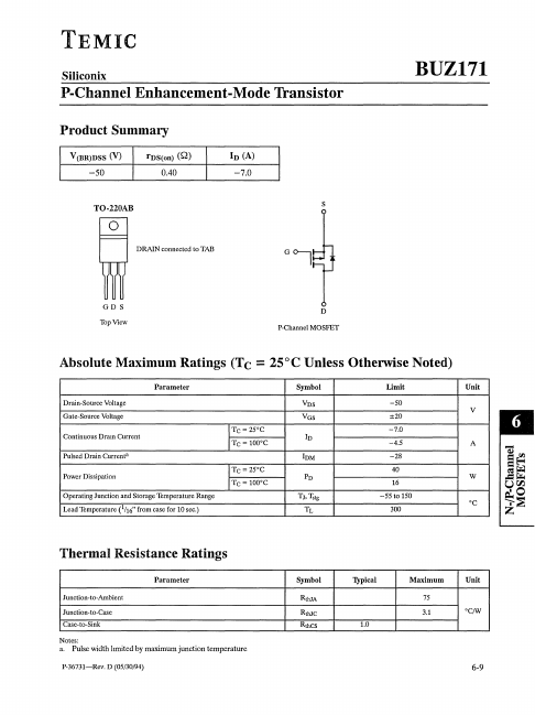
P-Channel Enhancement-Mode Transistor
Product Summary
V(BR)nSS (V)
-50
rnS(on) (Q) 0.40
In (A)
-7.0
TO·220AB
S
o
DRAIN connected to TAB
BUZ171
GDS Top View
D P-Channel MOSFET
Absolute Maximum Ratings (Tc = 25°C Unless Otherwise Noted)
Drain-Source Voltage Gate-Source Voltage
Parameter
Continuous Dram Current
Pulsed Drain Current'
Power Dissipation
Operating Junction and Storage Temperature Range
Lead Temperature (11t6" from case for 10 sec.)
ITc=25'C ITc = 100'C
LTC = 25'C ITc = 100'e
Symbol VDS VGS ID IDM PD
TJ,T,tg TL
Limit -50 ±20 -7.0 -4.5 -28 40 16 -55 to 150 300
Unit V
A W
'c
Thermal Resistance Ratings
Parameter Junction-la-Ambient Junction-la-Case Case-to-Sink
Notes:
a. Pulse width lImited by maximum junction temperature
P-36731-Rev.
 BUZ171 Datasheet