The following content is an automatically extracted verbatim text
from the original manufacturer datasheet and is provided for reference purposes only.
View original datasheet text
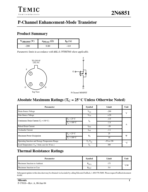
P-Channel Enhancement-Mode Transistor
Product Summary
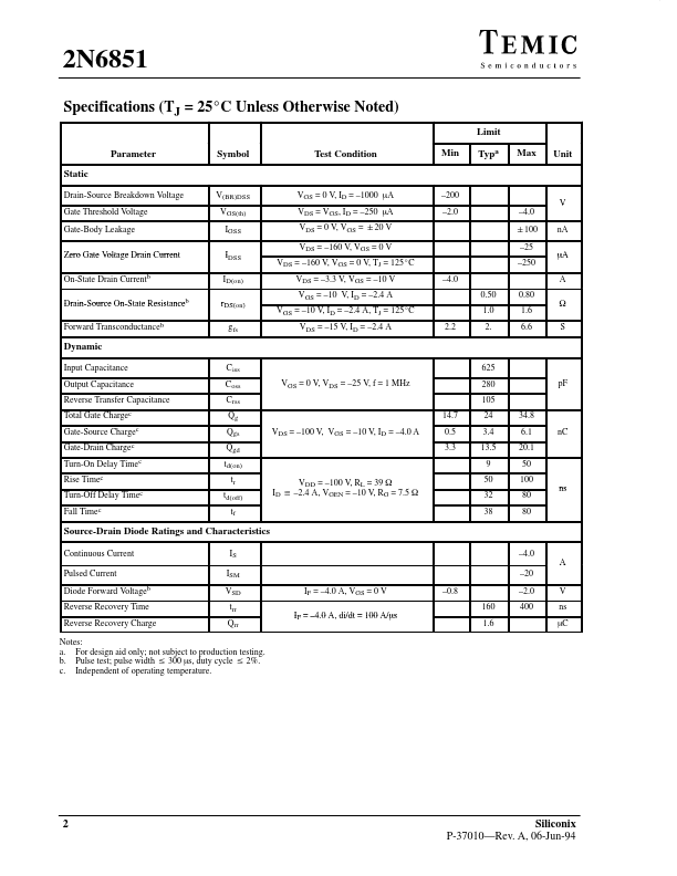
V(BR)DSS (V) –200
rDS(on) (W) 0.80
ID (A) –4.0
Parametric limits in accordance with MIL-S-19500/564 where applicable.
S
TO-205AF (TO-39)
S
G 1
2N6851
2 G
3 D
Top View
D P-Channel MOSFET
Absolute Maximum Ratings (TC = 25_C Unless Otherwise Noted)
Drain-Source Voltage Gate-Source Voltage
Parameter
Continuous Drain Current (TJ = 150_C)
Pulsed Drain Current Avalanche Current
Maximum Power Dissipation
Operating Junction and Storage Temperature Range Lead Temperature (1/16” from case for 10 sec.)
TC = 25_C TC = 100_C
TC = 25_C TC = 100_C
Thermal Resistance Ratings
Symbol VDS VGS
ID
IDM IAR
PD
TJ, Tstg TL
Limit
–200 "20 –4.0 –2.4 –20 –3.
 2N6851 Datasheet