SM7301
Description
The SM7301 is normally shipped with the on-chip FLASH memory array in the erased state (that is, contents = FFH) and ready to be programmed. To programming on-chip
FLASH memory, MCU must be in the RESET mode.
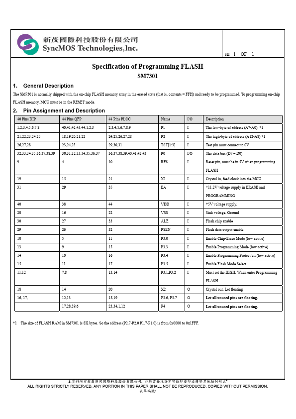
2. Pin Assignment and Description
40 Pins DIP
44 Pins QFP
44 Pins PLCC
Name
I/O Description
1,2,3,4,5,6,7,8
40,41,42,43,44,1,2,3
2,3,4,5,6,7,8,9
P1 I The low-byte of address (A7-A0),
- 1
21,22,23,24,25
18,19,20,21,22
24,25,26,27,28
P2 I The high-byte of address (A12-A8)
- 1
26,27,28
23,24,25
29,30,31
TST[1:3]
Test pin must connect to 0V
32,33,34,35,36,37,38,39 30,31,32,33,34,35,36,37 36,37,38,39,40,41,42,43
P0
I/O The data bus (D7
- D0)
RES I Reset pin, must be in 5V when programming
FLASH
19 15
X1 I Crystal in, feed clock into the MCU
31 29
EA I +11.2V voltage supply in ERASE and
PROGRAMMING...