Datasheet Details
| Part number | CXL5512M |
|---|---|
| Manufacturer | Sony Semiconductor Solutions |
| File Size | 158.00 KB |
| Description | CMOS-CCD 1H Delay Line for NTSC |
| Datasheet |
 CXL5512M Datasheet CXL5512M Datasheet
|
|
|
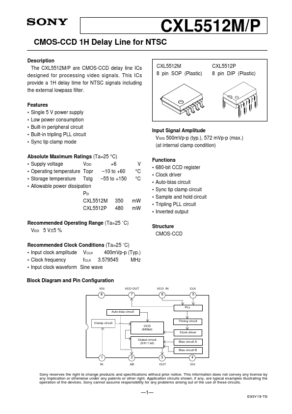
The CXL5512M/P are CMOS-CCD delay line ICs designed for processing video signals.
This ICs provide a 1H delay time for NTSC signals including the external lowpass filter.
| Part number | CXL5512M |
|---|---|
| Manufacturer | Sony Semiconductor Solutions |
| File Size | 158.00 KB |
| Description | CMOS-CCD 1H Delay Line for NTSC |
| Datasheet |
CXL5512M Datasheet
|
|
|
|
| Part Number | Description | Manufacturer |
|---|---|---|
| CXL02TG3 | HIGH PERFORMANCE ACCELEROMETER | ACEINNA |
| CXL04GP1 | GENERAL PURPOSE ACCELEROMETER | ACEINNA |
| CXL04GP3 | GENERAL PURPOSE ACCELEROMETER | ACEINNA |
| CXL10GP1 | GENERAL PURPOSE ACCELEROMETER | ACEINNA |
| CXL10GP3 | GENERAL PURPOSE ACCELEROMETER | ACEINNA |
| Part Number | Description |
|---|---|
| CXL5512P | CMOS-CCD 1H Delay Line for NTSC |
| CXL5513M | CMOS-CCD 1H Delay Line for NTSC |
| CXL5513P | CMOS-CCD 1H Delay Line for NTSC |
| CXL5514M | CMOS-CCD 1H Delay Line for PAL |
| CXL5514P | CMOS-CCD 1H Delay Line for PAL |
The following content is an automatically extracted verbatim text from the original manufacturer datasheet and is provided for reference purposes only.