Click to expand full text
CXG1117K
Power Amplifier Module for JCDMA
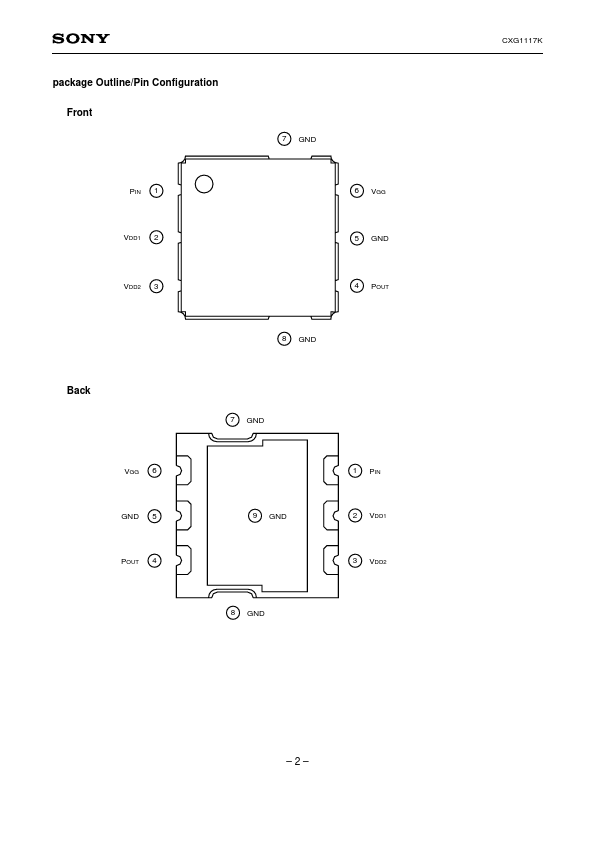
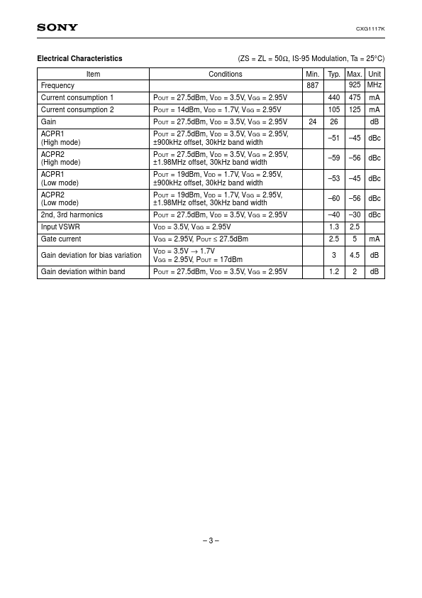
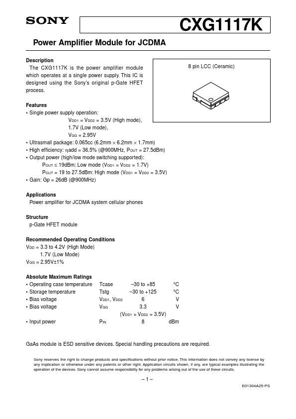
Description The CXG1117K is the power amplifier module which operates at a single power supply. This IC is designed using the Sony’s original p-Gate HFET process. Features • Single power supply operation: VDD1 = VDD2 = 3.5V (High mode), 1.7V (Low mode), VGG = 2.95V • Ultrasmall package: 0.065cc (6.2mm × 6.2mm × 1.7mm) • High efficiency: ηadd = 36.5% (@900MHz, POUT = 27.5dBm) • Output power (high/low mode switching supported): POUT ≤ 19dBm: Low mode (VDD1 = VDD2 = 1.7V) POUT = 19 to 27.5dBm: High mode (VDD1 = VDD2 = 3.5V) • Gain: Gp = 26dB (@900MHz) Applications Power amplifier for JCDMA system cellular phones Structure p-Gate HFET module Recommended Operating Conditions VDD = 3.3 to 4.2V (High Mode) 1.7V (Low Mode) VGG = 2.
 CXG1117K Datasheet