Click to expand full text
www.DataSheet4U.com
E L E C T R O N I C
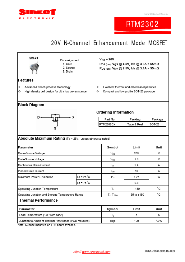
RTM2302
20V N-Channel Enhancement Mode MOSFET
Pin assignment: 1. Gate 2. Source 3. Drain
VDS = 20V RDS (on), Vgs @ 4.5V, Ids @ 3.6A = 65mΩ RDS (on), Vgs @ 2.5V, Ids @ 3.1A = 95mΩ
Features
Advanced trench process technology High density cell design for ultra low on-resistance Excellent thermal and electrical capabilities Compact and low profile SOT-23 package
Block Diagram Ordering Information
Part No. RTM2302CX Packing Tape & Reel Package SOT-23
Absolute Maximum Rating (Ta = 25℃
Parameter
Drain-Source Voltage Gate-Source Voltage Continuous Drain Current Pulsed Drain Current Maximum Power Dissipation
unless otherwise noted)
Symbol
VDS VGS ID IDM Ta = 25 C Ta = 75 C
o o
Limit
20V ±8 2.4 10 1.25 0.
 RTM2302 Datasheet