SP40N11DNJ
Feature
- High power and current handing capability
- Lead free product is acquired
- Surface mount package
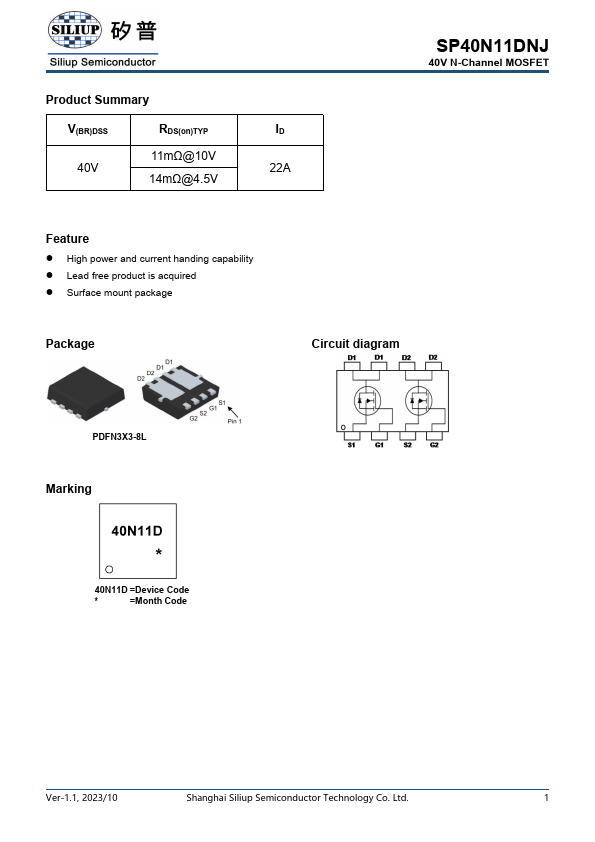
Package
Circuit diagram
PDFN3X3-8L
Marking
40N11D =Device Code
- =Month Code
Ver-1.1, 2023/10
Shanghai Siliup Semiconductor Technology Co. Ltd.
Absolute maximum ratings (Ta=25℃ unless otherwise noted)
Parameter
Symbol
Drain-Source Voltage
Gate-Source Voltage
Drain Current-Continuous
Pulsed Drain Current
Maximum Power Dissipation
Single Pulse Avalanche Energy1
Thermal Resistance,Junction-to-Ambient Operating Junction and Storage Temperature Range
RθJA TJ,TSTG
40V N-Channel MOSFET
Limit 40 ±20 22 88 26 20 4.8
-55 To 150
Unit V V A A W m J
℃/W ℃
Electrical characteristics (TA=25 o C, unless otherwise noted)
Parameter
Symbol
Condition
Min...