Click to expand full text
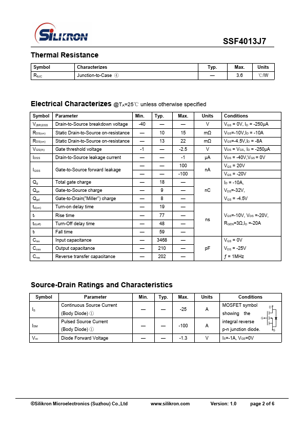
Main Product Characteristics:
VDSS
-40V
RDS(on) ID
10mΩ (typ.) -25A ①
PDFN 5x6-8L
SSF4013J7
Pin Assignments
Schematic Diagram
Features and Benefits:
Advanced MOSFET process technology Special designed for PWM, load switching and
general purpose applications Ultra low on-resistance with low gate charge Fast switching and reverse body recovery 150℃ operating temperature
Description:
It utilizes the latest processing techniques to achieve the high cell density and reduces the on-resistance with high repetitive avalanche rating. These features combine to make this design an extremely efficient and reliable device for use in power switching application and a wide variety of other applications.
 SSF4013J7 Datasheet