SMT002NA4G1
Features and Benefits
- Advanced MOSFET process technology
- Special designed for PWM, load switching and general purpose applications
- Ultra low on-resistance with low gate charge
- Fast switching and reverse body recovery
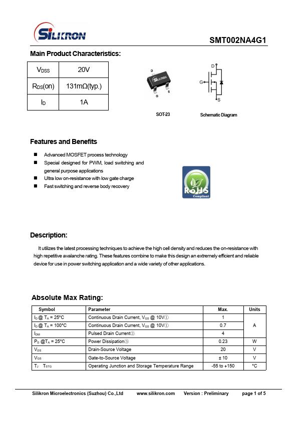
Schematic Diagram
Description
:
It utilizes the latest processing techniques to achieve the high cell density and reduces the on-resistance with high repetitive avalanche rating. These features bine to make this design an extremely efficient and reliable device for use in power switching application and a wide variety of other applications.
Absolute Max Rating:
Symbol ID @ TA = 25°C ID @ TA = 100°C IDM PD @TA = 25°C VDS VGS TJ TSTG
Parameter Continuous Drain Current, VGS @ 10V① Continuous Drain Current, VGS @ 10V① Pulsed Drain Current② Power Dissipation③ Drain-Source Voltage Gate-to-Source Voltage Operating Junction and Storage Temperature Range
Max. 1 0.7 4
0.23 20 ± 10 -55 to +150
Units
W V V °C
Silikron Microelectronics (Suzhou)...