Click to expand full text
monolithic dual n-channel JFETs designed for • • •
• DiHerential Amplifiers
H
Siliconix
Performance Curves NNR See Section 4
BENEFITS
• Minimum System Error and Calibration 5 mV Offset Maximum (2N3921)
• Simplifies Amplifier Design Low Output Conductance
TO-71 See Section 6
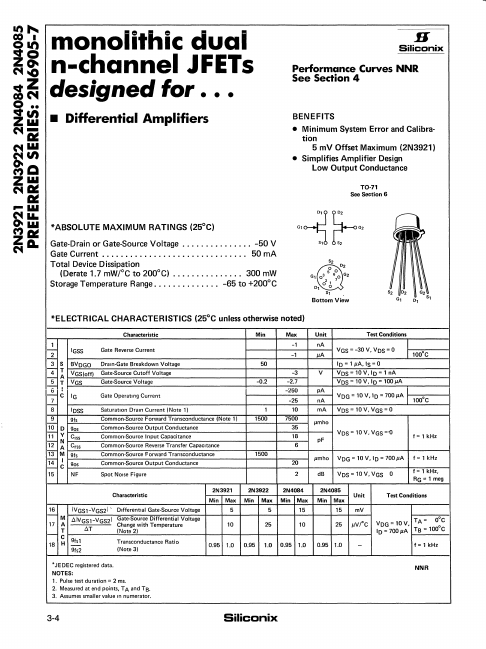
*ABSOLUTE MAXIMUM RATINGS (25°C)
Gate-Drain or Gate-Source Voltage ..............• -50 V Gate Current ............................... 50 rnA Total Device Dissipation
(Derate 1.7 mW;oC to 200°C) ..•............ 300mW Storage Temperature Range •............. -65 to +200°C
~~G1 G2 81 S2
o'2 02
.,5 0
G, 0 3 6 0 27
0, 00'
G2
Bottom View
l~G.0, '•
*ELECTRICAL CHARACTERISTICS (25°C unless otherwise noted)
Characteristic
.2. ~2 s
4"T -::-A
~:
-"b -c• ...l...
 2N4085 Datasheet