SW20N50D
Features
- Low gate charge
- 100% avalanche tested
- Improved dv/dt capability
- Ro HS pliant
- JEDEC Qualification
N-channel MOSFET BVDSS 500V ID 20A RDS(on) < 0.3W
Device SW20N50D
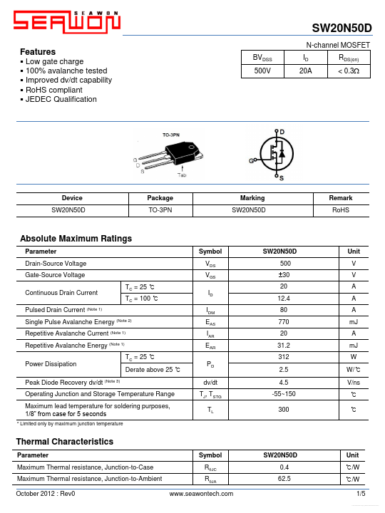
Package TO-3PN
Marking SW20N50D
Remark Ro HS
Absolute Maximum Ratings
Parameter Drain-Source Voltage Gate-Source Voltage Continuous Drain Current Pulsed Drain Current (Note 1) Single Pulse Avalanche Energy (Note 2) Repetitive Avalanche Current (Note 1) Repetitive Avalanche Energy (Note 1) Power Dissipation Peak Diode Recovery dv/dt (Note 3) Operating Junction and Storage Temperature Range Maximum lead temperature for soldering purposes, 1/8” from case for 5 seconds
- Limited only by maximum junction temperature
Symbol VDS VGS TC = 25 ℃ TC = 100 ℃ ID IDM EAS IAR EAR TC = 25 ℃ Derate above 25 ℃ PD dv/dt TJ, TSTG TL
SW20N50D 500 ±30 20 12.4 80 770 20 31.2 312 2.5 4.5 -55~150 300
Unit V V A A A m J A m J W W/℃ V/ns ℃ ℃
Thermal Characteristics
Parameter Maximum Thermal resistance, Junction-to-Case Maximum...