Click to expand full text
Elektronische Bauelemente
SSG4957
-7.7A, -30V,RDS(ON) 24m P-Channel Enhancement Mode Power Mos.FET
RoHS Compliant Product
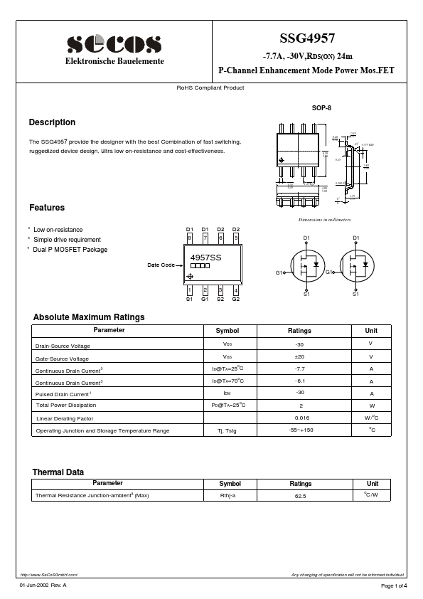
Description
The SSG4957 provide the designer with the best Combination of fast switching, ruggedized device design, ultra low on-resistance and cost-effectiveness.
Features
* Low on-resistance * Simple drive requirement * Dual P MOSFET Package
D1 D1 D2 D2 8 765
Date Code
4957SS
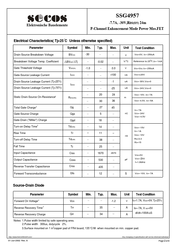
Absolute Maximum Ratings
Parameter
Drain-Source Voltage Gate-Source Voltage Continuous Drain Current3 Continuous Drain Current3 Pulsed Drain Current 1 Total Power Dissipation Linear Derating Factor Operating Junction and Storage Temperature Range
123 4 S1 G1 S2 G2
Symbol VDS VGS
ID@TA=25oC ID@TA=70oC
IDM PD@TA=25oC
Tj, Tstg
SOP-8
0.40 0.90
6.20 5.80
0.25
0.19 0.25
o
45 0.375 REF
3.
 SSG4957 Datasheet