With TO-3 package
High power dissipation APPLICATIONS
Power amplifier applications
Power switching applications
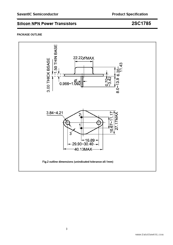
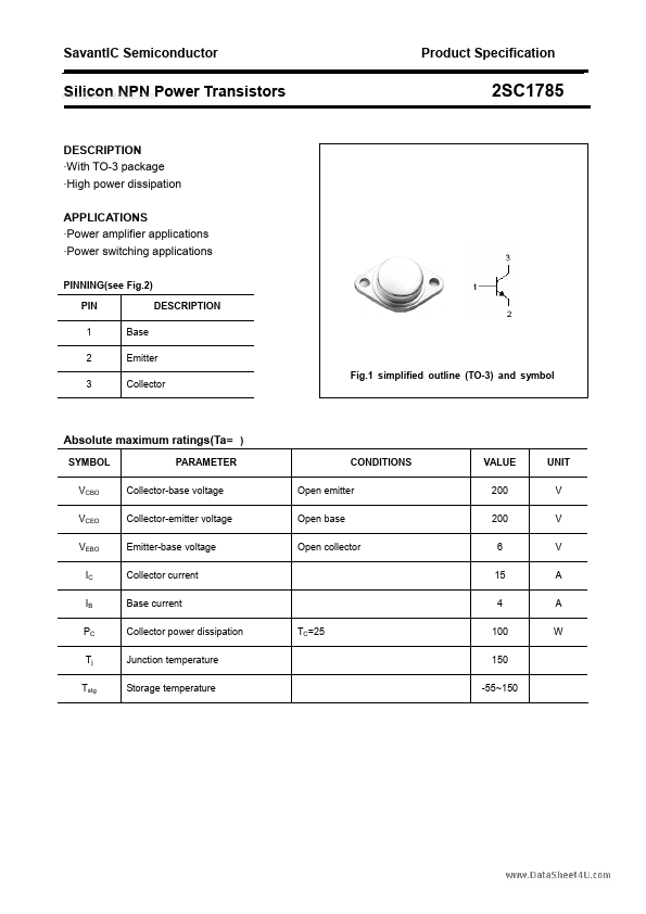
PINNING(see Fig.2) PIN 1 2 3 Base Emitter Collector Fig.1 simplified outline (TO-3) and symbol DESCRIPTION
Absolute maximum ratings(Ta= )
SYMBOL VCBO VCEO VEBO IC IB P
The following content is an automatically extracted verbatim text
from the original manufacturer datasheet and is provided for reference purposes only.
View original datasheet text
SavantIC Semiconductor
www.DataSheet4U.com
Product Specification
Silicon NPN Power Transistors
2SC1785
DESCRIPTION ·With TO-3 package ·High power dissipation APPLICATIONS ·Power amplifier applications ·Power switching applications
PINNING(see Fig.2) PIN 1 2 3 Base Emitter Collector Fig.1 simplified outline (TO-3) and symbol DESCRIPTION
Absolute maximum ratings(Ta= )
SYMBOL VCBO VCEO VEBO IC IB PC Tj Tstg PARAMETER Collector-base voltage Collector-emitter voltage Emitter-base voltage Collector current Base current Collector power dissipation Junction temperature Storage temperature TC=25 CONDITIONS Open emitter Open base Open collector VALUE 200 200 6 15 4 100 150 -55~150 UNIT V V V A A W
SavantIC Semiconductor
www.DataSheet4U.
 2SC1785 Datasheet