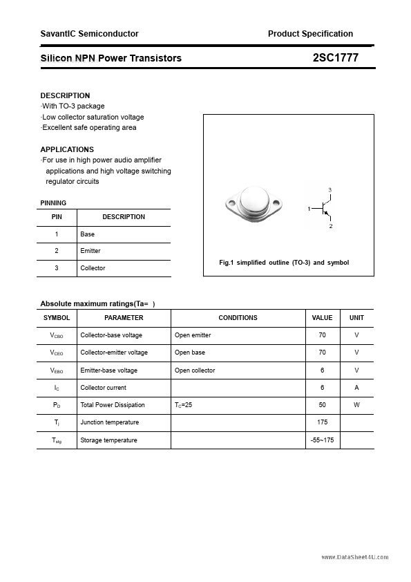
With TO-3 package
Low collector saturation voltage
Excellent safe operating area APPLICATIONS
For use in high power audio amplifier applications and high voltage switching regulator circuits
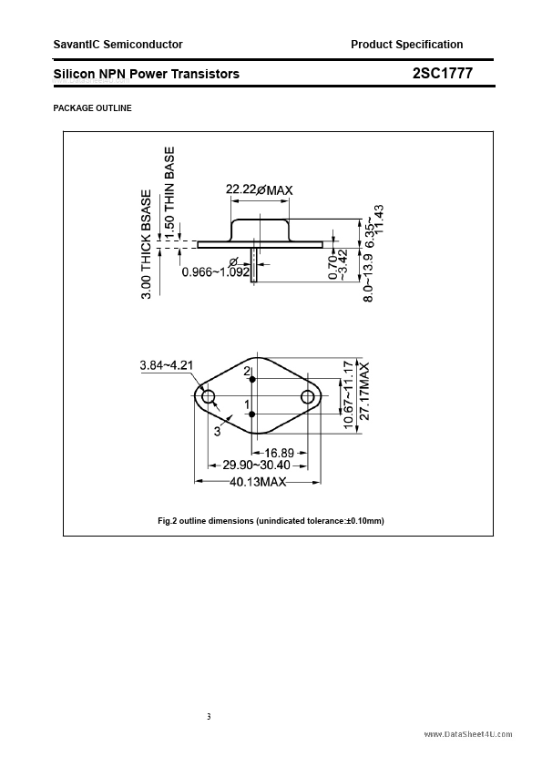
PINNING PIN 1 2 3 Base Emitter Collector Fig.1 simplified outline (TO-3) and symbol DESCR
The following content is an automatically extracted verbatim text
from the original manufacturer datasheet and is provided for reference purposes only.
View original datasheet text
SavantIC Semiconductor
www.DataSheet4U.com
Product Specification
Silicon NPN Power Transistors
2SC1777
DESCRIPTION ·With TO-3 package ·Low collector saturation voltage ·Excellent safe operating area APPLICATIONS ·For use in high power audio amplifier applications and high voltage switching regulator circuits
PINNING PIN 1 2 3 Base Emitter Collector Fig.1 simplified outline (TO-3) and symbol DESCRIPTION
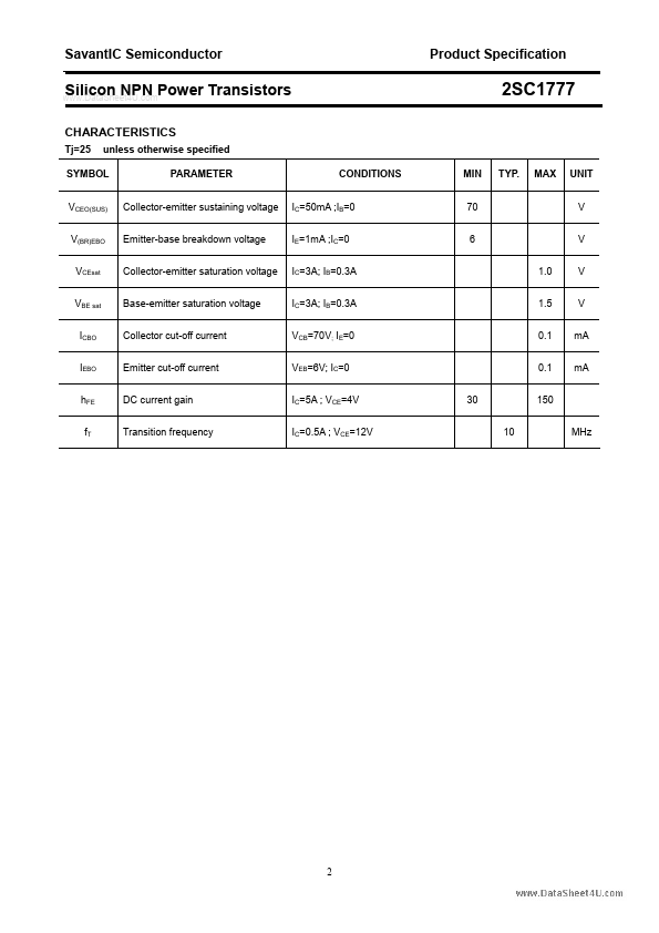
Absolute maximum ratings(Ta= )
SYMBOL VCBO VCEO VEBO IC PD Tj Tstg PARAMETER Collector-base voltage Collector-emitter voltage Emitter-base voltage Collector current Total Power Dissipation Junction temperature Storage temperature TC=25 Open emitter Open base Open collector CONDITIONS VALUE 70 70 6 6 50 175 -55~175 UNIT V V V A W
SavantIC Semiconductor
www.DataSheet4U.
 2SC1777 Datasheet