The following content is an automatically extracted verbatim text
from the original manufacturer datasheet and is provided for reference purposes only.
View original datasheet text
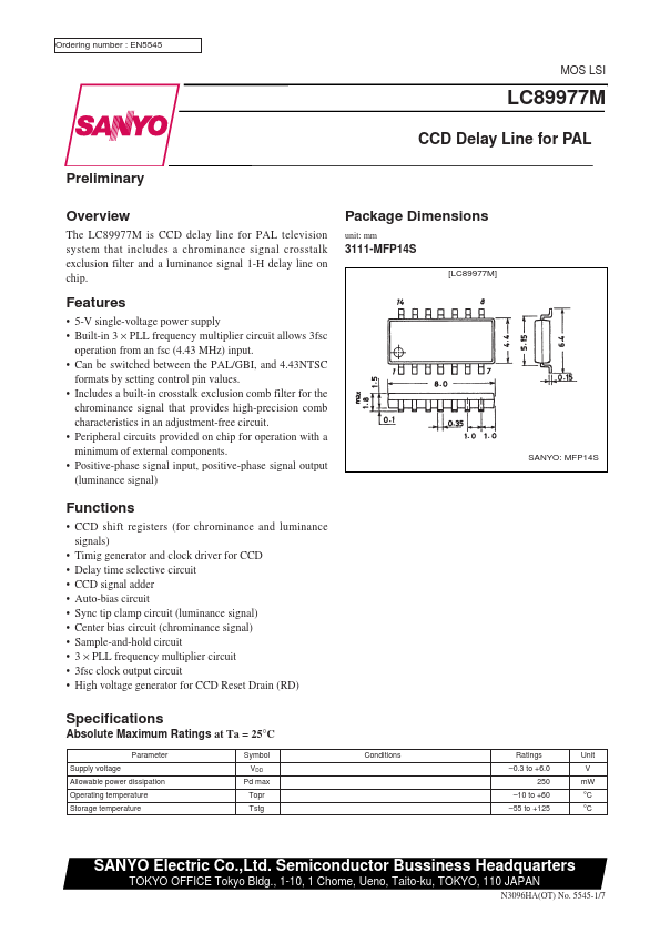
Ordering number : EN5545
MOS LSI
LC89977M
CCD Delay Line for PAL
Preliminary Overview
The LC89977M is CCD delay line for PAL television system that includes a chrominance signal crosstalk exclusion filter and a luminance signal 1-H delay line on chip.
Package Dimensions
unit: mm
3111-MFP14S
[LC89977M]
Features
• 5-V single-voltage power supply • Built-in 3 × PLL frequency multiplier circuit allows 3fsc operation from an fsc (4.43 MHz) input. • Can be switched between the PAL/GBI, and 4.43NTSC formats by setting control pin values. • Includes a built-in crosstalk exclusion comb filter for the chrominance signal that provides high-precision comb characteristics in an adjustment-free circuit. • Peripheral circuits provided on chip for operation with a minimum of external components.
 LC89977M Datasheet