The following content is an automatically extracted verbatim text
from the original manufacturer datasheet and is provided for reference purposes only.
View original datasheet text
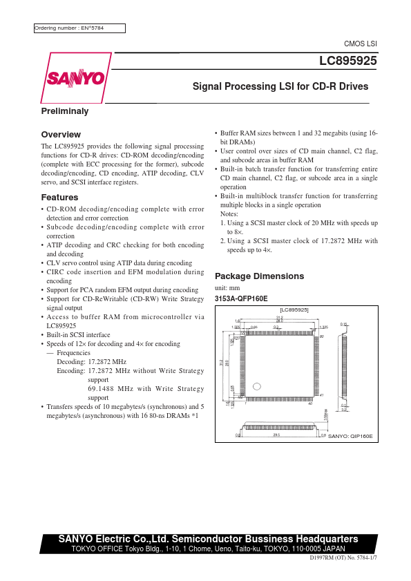
Ordering number : EN*5784
CMOS LSI
LC895925
Signal Processing LSI for CD-R Drives
Preliminaly Overview
The LC895925 provides the following signal processing functions for CD-R drives: CD-ROM decoding/encoding (complete with ECC processing for the former), subcode decoding/encoding, CD encoding, ATIP decoding, CLV servo, and SCSI interface registers. • Buffer RAM sizes between 1 and 32 megabits (using 16bit DRAMs) • User control over sizes of CD main channel, C2 flag, and subcode areas in buffer RAM • Built-in batch transfer function for transferring entire CD main channel, C2 flag, or subcode area in a single operation • Built-in multiblock transfer function for transferring multiple blocks in a single operation Notes: 1. Using a SCSI master clock of 20 MHz with speeds up to 8×. 2.
 LC895925 Datasheet