Description
Pin name VSS1,2 VDD1,2 VP PORT0 P00 to P07 I/O I/O Power pin (+)
1 Function description Power pin (-) Short-circuit VSS1 to VSS2.
8-bit input/output port
Input for port 0 interrupt
Input/output in nibb
Features
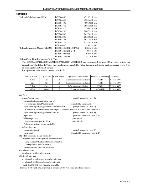
- (1) Read-Only Memory (ROM) : LC866448B 49152 × 8 bits : LC866444B 45056 × 8 bits : LC866440B 40960 × 8 bits : LC866436B 36864 × 8 bits : LC866432B 32768 × 8 bits : LC866428B 28672 × 8 bits : LC866424B 24576 × 8 bits : LC866420B 20480 × 8 bits : LC866416B 16384 × 8 bits : LC866412B 12288 × 8 bits : LC866408B 8192 × 8 bits (2) Random Access Memory (RAM) : LC866448B/44B/40B/36B 1152 × 8 bits : LC866432B/28B/24B 768 × 8 bits : LC866420B/16B 640 × 8 bits : LC866412B/08B 512 × 8 bits (3) Bus Cycle Tim.
 LC866408B Datasheet