C3917
Features
- On-chip bias resistance : R1=4.7kΩ, R2=4.7kΩ.
- Small-sized package : SPA.
- Large current capacity : IC=500m A.
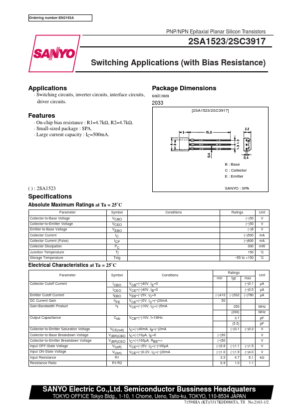
Package Dimensions unit:mm 2033
[2SA1523/2SC3917]
( ) : 2SA1523
Specifications
Absolute Maximum Ratings at Ta = 25˚C
Parameter Collector-to-Base Voltage Collector-to-Emitter Voltage Emitter-to-Base Voltage Collector Current Collector Current (Pulse) Collector Dissipation Junction Temperature Storage Temperature
Symbol
VCBO VCEO VEBO
IC ICP PC Tj
Tstg
Electrical Characteristics at Ta = 25˚C
Conditions
Parameter Collector Cutoff Current
Emitter Cutoff Current DC Current Gain Gain-Bandwidth Product
Symbol
Conditions
ICBO ICEO IEBO h FE f T
VCB=(- )40V, IE=0 VCE=(- )40V, IB=0 VEB=(- )5V, IC=0 VCE=(- )5V, IC=(- )20m A VCE=(- )10V, IC=(- )5m A
Output Capacitance
Cob VCB=(- )10V, f=1MHz
Collector-to-Emitter Saturation Voltage Collector-to-Base Breakdown Voltage Collector-to-Emitter Breakdown Voltage Input OFF-State Voltage Input ON-State Voltage Input Resistance...