Datasheet4U Logo Datasheet4U.com

K7D801871B - SRAM

Download the K7D801871B datasheet PDF. This datasheet also covers the K7D803671B variant, as both devices belong to the same sram family and are provided as variant models within a single manufacturer datasheet.

General Description

Pin Name K, K SA SA0, SA1 DQ VDD VDDQ VREF B1 B2 B3 Pin Description Differential Clocks Synchronous Address Input Synchronous Burst Address Input (SA0 = LSB) Synchronous Data I/O Core Power Supply Output Power Supply HSTL Input Reference Voltage Load External Address Burst R/W Enable Single/Double

Key Features

  • 256Kx36 or 512Kx18 Organizations.
  • 153(9x17) Pin Ball Grid Array Package(14mm x 22mm).
  • Programmable Impedance Output Drivers.
  • Maximum Frequency : 333MHz (Data Rate : 666Mbps).
  • 2.5V Core/1.5V Output Power Supply(2.0V max VDDQ).
  • HSTL Input and Outputs.
  • Single Differential HSTL Clock. Organization.
  • Synchronous Pipeline Mode of Operation with Self-Timed Late Write. Part Number Maximum Access Frequency Time.

📥 Download Datasheet

Note: The manufacturer provides a single datasheet file (K7D803671B-Samsung.pdf) that lists specifications for multiple related part numbers.

Full PDF Text Transcription for K7D801871B (Reference)

Note: Below is a high-fidelity text extraction (approx. 800 characters) for K7D801871B. For precise diagrams, and layout, please refer to the original PDF.

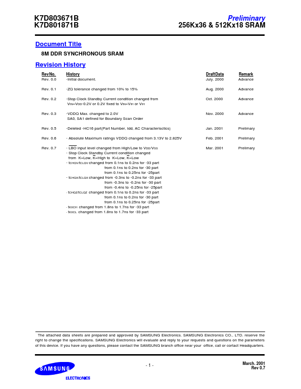
K7D803671B K7D801871B Preliminary 256Kx36 & 512Kx18 SRAM Document Title 8M DDR SYNCHRONOUS SRAM Revision History Rev No. Rev. 0.0 History -Initial document. Rev. 0.1 -ZQ ...

View more extracted text
sion History Rev No. Rev. 0.0 History -Initial document. Rev. 0.1 -ZQ tolerance changed from 10% to 15% Rev. 0.2 -Stop Clock Standby Current condition changed from VIN=VDD-0.2V or 0.2V fixed to VIN=VIH or VIH Rev. 0.3 -VDDQ Max. changed to 2.0V SA0, SA1 defined for Boundary Scan Order Rev. 0.5 -Deleted -HC16 part(Part Number, Idd, AC Characterisctics) Rev. 0.6 - Absolute Maximum ratings VDDQ changed from 3.13V to 2.825V Rev. 0.7 - LBO input level changed from High/Low to VDD/VSS - Stop Clock Standby Current condition changed from K=Low, K=High to K=Low, K=Low - tCHQV/tCLQV changed from 0.1ns to 0.2ns for -33 part from 0.1n