Datasheet Details
| Part number | K4T1G044QM |
|---|---|
| Manufacturer | Samsung Semiconductor |
| File Size | 457.24 KB |
| Description | 1Gb M-die DDR2 SDRAM Specification |
| Datasheet |
 K4T1G044QM Datasheet K4T1G044QM Datasheet
|
|
|
3.
4.
Rev.1.1 Jan.
| Part number | K4T1G044QM |
|---|---|
| Manufacturer | Samsung Semiconductor |
| File Size | 457.24 KB |
| Description | 1Gb M-die DDR2 SDRAM Specification |
| Datasheet |
K4T1G044QM Datasheet
|
|
|
|
Note: Below is a high-fidelity text extraction (approx. 800 characters) for K4T1G044QM. For precise diagrams, and layout, please refer to the original PDF.
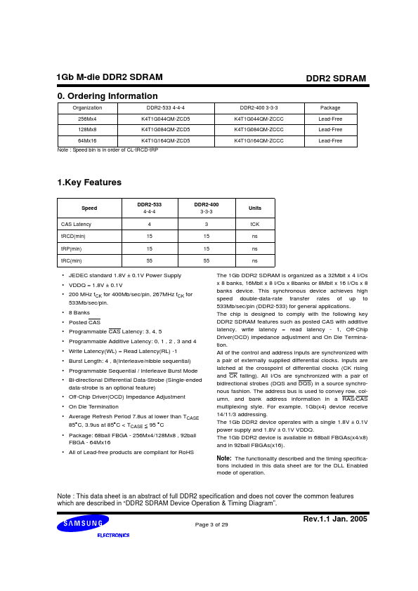
1Gb M-die DDR2 SDRAM DDR2 SDRAM 1Gb M-die DDR2 SDRAM Specification Version 1.1 January 2005 Page 1 of 29 Rev.1.1 Jan. 2005 1Gb M-die DDR2 SDRAM Contents DDR2 SDRAM 0. Ord...
| Brand Logo | Part Number | Description | Manufacturer |
|---|---|---|---|
| K4T1G044QA | 1Gb A-die DDR2 SDRAM Specification | Samsung semiconductor | |
| K4T1G044QA-ZCE6 | 1Gb A-die DDR2 SDRAM Specification | Samsung semiconductor | |
| K4T1G044QC | (K4T1G044QC / K4T1G084QC) 1Gb C-die DDR2 SDRAM Specification | Samsung semiconductor | |
| K4T1G044QE | 1Gb E-die DDR2 SDRAM | Samsung Electronics | |
| K4T1G044QQ | (K4T1G044QQ - K4T1G164QQ) 1Gb A-die DDR2 SDRAM Specification | Samsung semiconductor |
| Part Number | Description |
|---|---|
| K4T1G044QF | 1Gb F-die DDR2 SDRAM |
| K4T1G044QF-BCE6 | 1Gb F-die DDR2 SDRAM |
| K4T1G044QF-BCE7 | 1Gb F-die DDR2 SDRAM |
| K4T1G044QF-BCF7 | 1Gb F-die DDR2 SDRAM |
| K4T1G084QF | 1Gb F-die DDR2 SDRAM |
| K4T1G084QF-BCE6 | 1Gb F-die DDR2 SDRAM |
| K4T1G084QF-BCE7 | 1Gb F-die DDR2 SDRAM |
| K4T1G084QF-BCF7 | 1Gb F-die DDR2 SDRAM |
| K4T1G084QJ | 1Gb J-die DDR2 SDRAM |
| K4T1G164QF | 1Gb F-die DDR2 SDRAM |