S5C7221X01-V0T0 - TIMING & SYNC. GENERATOR FOR B/W CCD
Samsung Semiconductor
Description
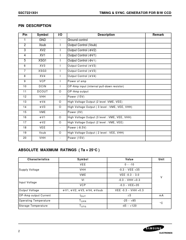
Pin 1 2 3 4 5
6 7 8 9 10 11 12 13 14 15 16 17 18 19 20
Symbol GND Xsub XV2 XV1 XSG1
XV3 XSG3 XV4 VCP DCIN DCOUT VHH
Φ V4 Φ V3
I/O I I I I
I I I I I O O O O O O -
Description Ground control Output Control (Vsub) Output Control ( ΦV2) Output Control ( ΦV1) Output Control ( ΦV1)
Output Control ( Φ V
Features
Includes voltage source circuit for CCD image sensor Input voltage : 5V / 3.3V Package : 20 SSOP.
The following content is an automatically extracted verbatim text
from the original manufacturer datasheet and is provided for reference purposes only.
View original datasheet text
TIMING & SYNC. GENERATOR FOR B/W CCD
S5C7221X01
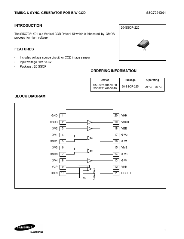
INTRODUCTION
The S5C7221X01 is a Vertical CCD Driver LSI which is fabricated by CMOS process for high voltage
20-SSOP-225
FEATURES
• • • Includes voltage source circuit for CCD image sensor Input voltage : 5V / 3.3V Package : 20 SSOP
ORDERING INFORMATION
Device S5C7221X01-V0B0 S5C7221X01-V0T0 Package 20-SSOP-225 Operating -20 °C − 85 °C
BLOCK DIAGRAM
GND XSUB XV2 XV1 XSG1 XV3 XSG3 XV4 VCP DCIN
1 2 3 4 5 6 7 8 9 10
20 19 18 17 16 15 14 13 12 11
VHH VSUB VEE Φ V2 Φ V1 VME Φ V3 Φ V4 VHH DCOUT
1
S5C7221X01
TIMING & SYNC.
 S5C7221X01-V0T0 Datasheet