Datasheet Details
| Part number | K7Q161854A |
|---|---|
| Manufacturer | Samsung Semiconductor |
| File Size | 389.08 KB |
| Description | (K7Q161854A / K7Q163654A) 1Mx18-bit QDR SRAM |
| Datasheet |
 K7Q161854A Datasheet K7Q161854A Datasheet
|
|
|
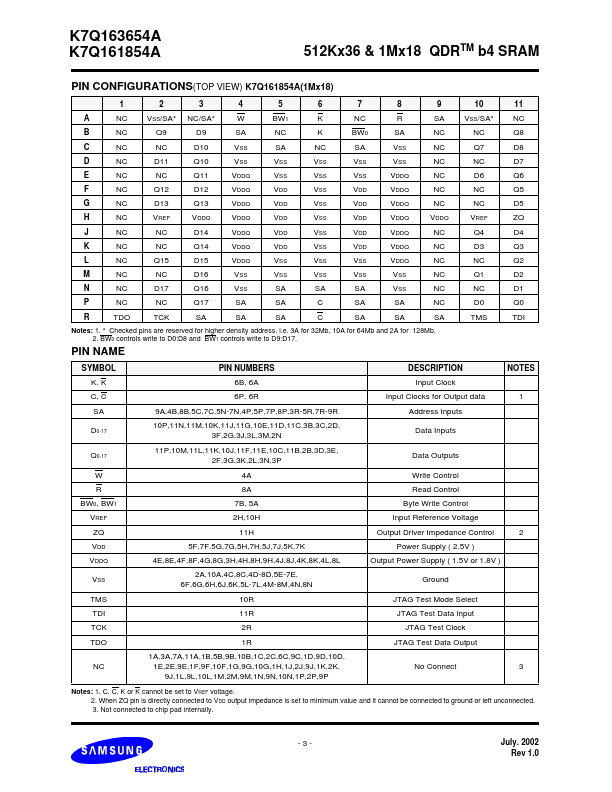
W (4A) : from Read Control Pin to Write Control R (8A) : from Write Control Pin to Read Control BW0(7B),BW1(7A),BW2(5A),BW3(5B) : from Read Control Pin to Byte Wrtie Control 2) Page 7 STATE DIAGRAM from LEAD NOP to READ NOP 1.
| Part number | K7Q161854A |
|---|---|
| Manufacturer | Samsung Semiconductor |
| File Size | 389.08 KB |
| Description | (K7Q161854A / K7Q163654A) 1Mx18-bit QDR SRAM |
| Datasheet |
K7Q161854A Datasheet
|
|
|
|
Note: Below is a high-fidelity text extraction (approx. 800 characters) for K7Q161854A. For precise diagrams, and layout, please refer to the original PDF.
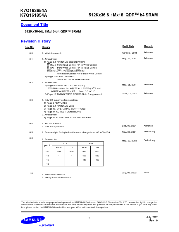
www.DataSheet4U.com K7Q163654A K7Q161854A Document Title 512Kx36-bit, 1Mx18-bit QDRTM SRAM 512Kx36 & 1Mx18 QDRTM b4 SRAM Revision History Rev. No. 0.0 0.1 History 1. Init...
| Part Number | Description |
|---|---|
| K7Q161852A | (K7Q161852A / K7Q163652A) 512Kx36 & 1Mx18 QDRTM b2 SRAM |
| K7Q161862B | (K7Q161862B / K7Q163662B) 512Kx36 & 1Mx18 QDRTM b2 SRAM |
| K7Q161864B | (K7Q161864B / K7Q163664B) 512Kx36 & 1Mx18 QDR TM b4 SRAM |
| K7Q161882A | (K7Q161882A / K7Q161882A) 512Kx36 & 1Mx18 QDR b2 SRAM |
| K7Q163652A | (K7Q161852A / K7Q163652A) 512Kx36 & 1Mx18 QDRTM b2 SRAM |
| K7Q163654A | (K7Q161854A / K7Q163654A) 1Mx18-bit QDR SRAM |
| K7Q163662B | (K7Q161862B / K7Q163662B) 512Kx36 & 1Mx18 QDRTM b2 SRAM |
| K7Q163664B | (K7Q161864B / K7Q163664B) 512Kx36 & 1Mx18 QDR TM b4 SRAM |
| K7Q163682A | (K7Q161882A / K7Q161882A) 512Kx36 & 1Mx18 QDR b2 SRAM |