Datasheet4U Logo Datasheet4U.com

K7P161866A - (K7P161866A / K7P163866A) 512Kx36 AND 1Mx18 Synchronous Pipelined SRAM

General Description

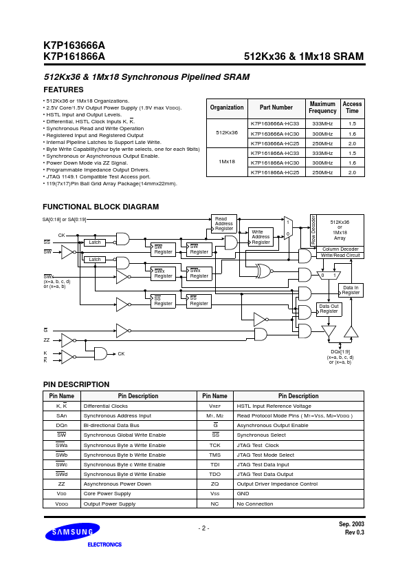
Pin Name K, K SAn DQn SW SWa SWb SWc SWd ZZ VDD VDDQ Pin Description Differential Clocks Synchronous Address Input Bi-directional Data Bus Synchronous Global Write Enable Synchronous Byte a Write Enable Synchronous Byte b Write Enable Synchronous Byte c Write Enable Synchronous Byte d Write Enable A

Key Features

  • 512Kx36 or 1Mx18 Organizations.
  • 2.5V Core/1.5V Output Power Supply (1.9V max VDDQ).
  • HSTL Input and Output Levels.
  • Differential, HSTL Clock Inputs K, K.
  • Synchronous Read and Write Operation.
  • Registered Input and Registered Output.
  • Internal Pipeline Latches to Support Late Write.
  • Byte Write Capability(four byte write selects, one for each 9bits).
  • Synchronous or Asynchronous Output Enable.
  • Power Down Mo.

📥 Download Datasheet

Full PDF Text Transcription for K7P161866A (Reference)

Note: Below is a high-fidelity text extraction (approx. 800 characters) for K7P161866A. For precise diagrams, and layout, please refer to the original PDF.

www.DataSheet4U.com K7P163666A K7P161866A Document Title 512Kx36 & 1Mx18 Synchronous Pipelined SRAM 512Kx36 & 1Mx18 SRAM Revision History Rev. No. Rev. 0.0 Rev. 0.1 Histo...

View more extracted text
512Kx36 & 1Mx18 SRAM Revision History Rev. No. Rev. 0.0 Rev. 0.1 History - Initial Document - Absolute maximum ratings are changed VDD : 2.815 - > 3.13 VDDQ : 2.815 - > 2.4 VTERM : 2.815 - > VDDQ+0.5 (2.4V MAX) - Recommended DC operating conditions are changed VREF / VCM-CLK : 0.68 - > 0.6, 0.95 - > 0.9 - DC characteristics is changed ISBZZ : 150 - > 128 - AC Characteristics are changed TAVKH / TDVKH / TWVKH / TSVKH : 0.4 / 0.5 / 0.5 - > 0.3 / 0.3 / 0.3 TKHAX / TKHDX / TKHWX / TKHSX : 0.5 / 0.5 / 0.5 - > 0.5 / 0.6 / 0.6 Draft Date Dec. 2001 Oct. 2002 Remark Advance Advance Rev. 0.2 - Recommended DC operating condition is c