Datasheet Details
| Part number | K4X51323PC-7E |
|---|---|
| Manufacturer | Samsung Semiconductor |
| File Size | 287.19 KB |
| Description | 16M x32 Mobile-DDR SDRAM |
| Datasheet |
 K4X51323PC-7E Datasheet K4X51323PC-7E Datasheet
|
|
|
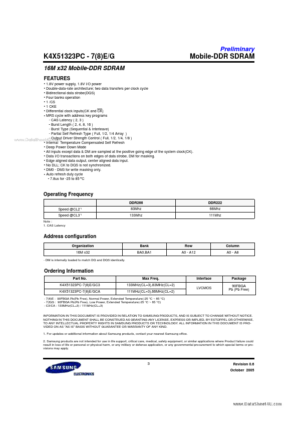
Clock : CK and CK are differential clock inputs.
All address and control input signals are sampled on the crossing of the positive edge of CK and negative edge of CK.
Internal clock signals are derived from CK/CK.
| Part number | K4X51323PC-7E |
|---|---|
| Manufacturer | Samsung Semiconductor |
| File Size | 287.19 KB |
| Description | 16M x32 Mobile-DDR SDRAM |
| Datasheet |
K4X51323PC-7E Datasheet
|
|
|
|
Note: Below is a high-fidelity text extraction (approx. 800 characters) for K4X51323PC-7E. For precise diagrams, and layout, please refer to the original PDF.
Preliminary K4X51323PC - 7(8)E/G Mobile-DDR SDRAM www.DataSheet4U.com 16M x32 Mobile-DDR SDRAM 1 Revision 0.6 October 2005 Preliminary K4X51323PC - 7(8)E/G Document Title...
| Part Number | Description |
|---|---|
| K4X51323PC-7G | 16M x32 Mobile-DDR SDRAM |
| K4X51323PC-8E | 16M x32 Mobile-DDR SDRAM |
| K4X51323PC-8G | 16M x32 Mobile-DDR SDRAM |
| K4X51163PC | 32M x16 Mobile-DDR SDRAM |
| K4X51163PC-FE | 32M x16 Mobile-DDR SDRAM |
| K4X51163PC-FG | 32M x16 Mobile-DDR SDRAM |
| K4X51163PC-LE | 32M x16 Mobile-DDR SDRAM |
| K4X51163PC-LG | 32M x16 Mobile-DDR SDRAM |
| K4X51163PE-FG | 32Mx16 Mobile DDR SDRAM |
| K4X51163PE-LE | 32Mx16 Mobile DDR SDRAM |