SP8256
FEATURES
Super high dense cell design for low R DS(ON). Rugged and reliable. Suface Mount Package. ESD Protected.
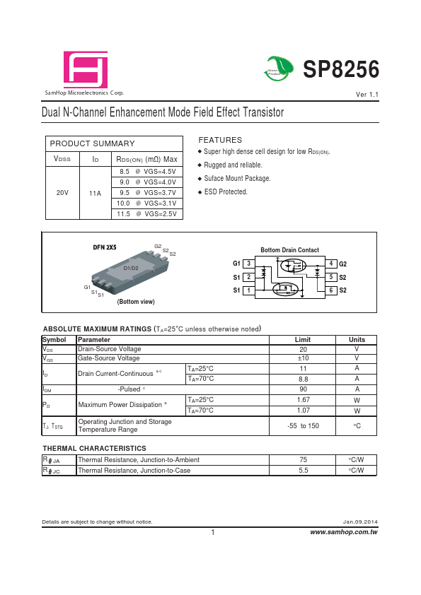
DF N 2X5
G2
S2
S2
Bottom Drain Contact
D1/D2
G1 S1
3 2 1
4 G2 5 6 S2 S2
G1 S1 S1
S1
(Bottom view)
ABSOLUTE MAXIMUM RATINGS ( T A=25 °C unless otherwise noted ) Symbol VDS VGS ID IDM PD TJ, TSTG Parameter Drain-Source Voltage Gate-Source Voltage Drain Current-Continuous -Pulsed c ac
Limit 20 ±10 TA=25°C TA=70°C TA=25°C TA=70°C 11 8.8 90 a
Units V V A A A W W °C
Maximum Power Dissipation
1.67 1.07 -55 to 150
Operating Junction and Storage Temperature Range
THERMAL CHARACTERISTICS R JA R JC Thermal Resistance, Junction-to-Ambient Thermal Resistance, Junction-to-Case 75 5.5 °C/W °C/W
Details are subject to change without notice.
Jan,09,2014
.samhop..tw
Ver 1.1
ELECTRICAL CHARACTERISTICS ( T A=25 °C unless otherwise noted )
Symbol Parameter Conditions
VGS=0V , ID=250u A VDS=16V , VGS=0V
Min 20
Typ
Max
Units
OFF CHARACTERISTICS Drain-Source...