Click to expand full text
SDT03N04Green
Product
Sa mHop Microelectronics C orp.
N-Channel Enhancement Mode Field Effect Transistor
Ver 1.2
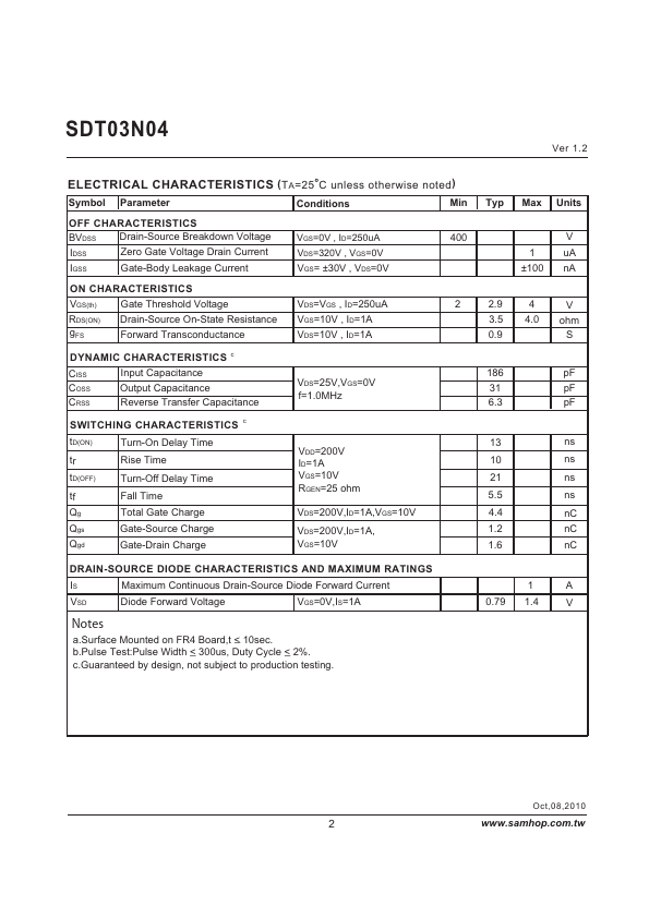
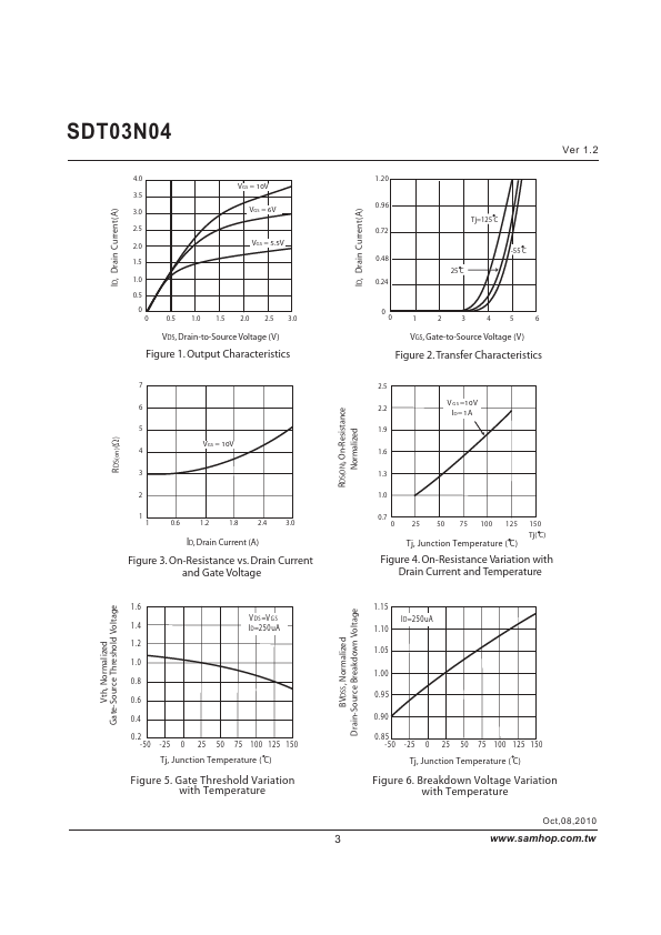
PRODUCT SUMMARY
VDSS
ID RDS(ON) (Ω) Typ
400V
1.5A
3.5 @ VGS=10V
F E AT UR E S S uper high dense cell design for low R DS(ON).
R ugged and reliable. S urface Mount P ackage.
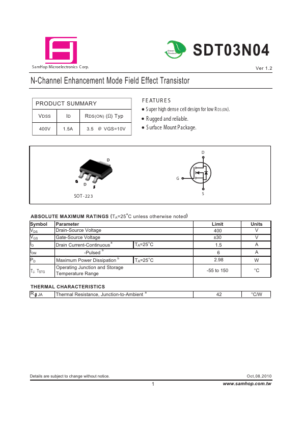
D
G S
SOT - 22 3
G S
ABSOLUTE MAXIMUM RATINGS (TA=25°C unless otherwise noted)
Symbol Parameter
VDS Drain-Source Voltage VGS Gate-Source Voltage ID Drain Current-Continuous a
TA=25°C
IDM -Pulsed b
PD
Maximum Power Dissipation b
TA=25°C
TJ, TSTG
Operating Junction and Storage Temperature Range
THERMAL CHARACTERISTICS
R JA
Thermal Resistance, Junction-to-Ambient a
Limit 400 ±30 1.5
6 2.98 -55 to 150
42
Units V V A A W °C
°C/W
Details are subject to change without notice.
 SDT03N04 Datasheet