Datasheet Details
| Part number | SPP3413W |
|---|---|
| Manufacturer | SYNC POWER |
| File Size | 340.10 KB |
| Description | P-Channel MOSFET |
| Datasheet |
 SPP3413W Datasheet SPP3413W Datasheet
|
|
|
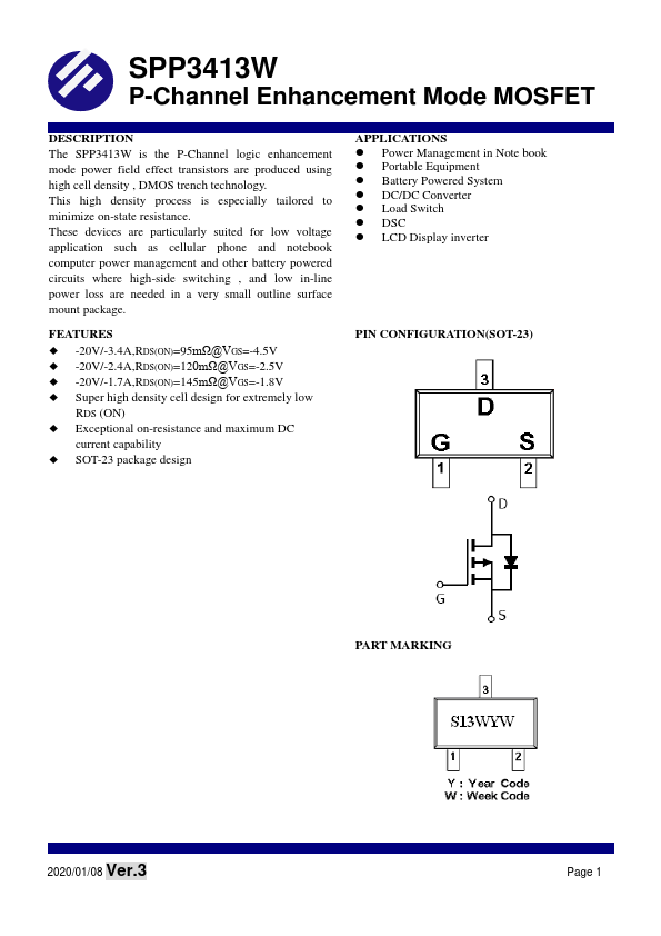
The SPP3413W is the P-Channel logic enhancement mode power field effect transistors are produced using high cell density , DMOS trench technology.
This high density process is especially tailored to minimize on-state resistance.
| Part number | SPP3413W |
|---|---|
| Manufacturer | SYNC POWER |
| File Size | 340.10 KB |
| Description | P-Channel MOSFET |
| Datasheet |
SPP3413W Datasheet
|
|
|
|
| Part Number | Description | Manufacturer |
|---|---|---|
| SPP30N03 | SIPMOS Power Transistor | Infineon Technologies |
| SPP30N10 | SIPMOS Power Transistor | Infineon Technologies |
| SPP-250-LLPL | Coaxial Cables | TMC |
| SPP-375-LLPL | Coaxial Cables | TMC |
| SPP-500-LLPL | Coaxial Cables | TMC |
| Part Number | Description |
|---|---|
| SPP3413 | P-Channel MOSFET |
| SPP3401 | P-Channel MOSFET |
| SPP3401B | P-Channel MOSFET |
| SPP3401D | P-Channel MOSFET |
| SPP3401W | P-Channel MOSFET |
The following content is an automatically extracted verbatim text from the original manufacturer datasheet and is provided for reference purposes only.