Datasheet Details
| Part number | STW8NC70Z |
|---|---|
| Manufacturer | STMicroelectronics |
| File Size | 199.85 KB |
| Description | N-CHANNEL ENHANCEMENT MODE POWER MOS TRANSISTORS |
| Datasheet |
 STW8NC70Z Datasheet STW8NC70Z Datasheet
|
|
|
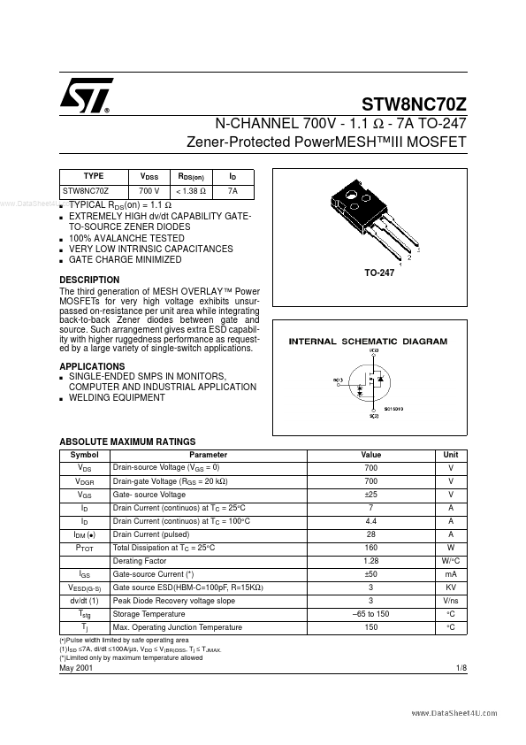
The third generation of MESH OVERLAY ™ Power MOSFETs for very high voltage exhibits unsurpassed on-resistance per unit area while integrating back-to-back Zener diodes between gate and source.
| Part number | STW8NC70Z |
|---|---|
| Manufacturer | STMicroelectronics |
| File Size | 199.85 KB |
| Description | N-CHANNEL ENHANCEMENT MODE POWER MOS TRANSISTORS |
| Datasheet |
STW8NC70Z Datasheet
|
|
|
|