Datasheet Details
| Part number | STCD1030 |
|---|---|
| Manufacturer | STMicroelectronics |
| File Size | 1.78 MB |
| Description | Multi-channel clock distribution circuit |
| Datasheet |
 STCD1030 Datasheet STCD1030 Datasheet
|
|
|
Download the STCD1030 datasheet PDF. This datasheet also covers the STCD1020 variant, as both devices belong to the same multi-channel clock distribution circuit family and are provided as variant models within a single manufacturer datasheet.
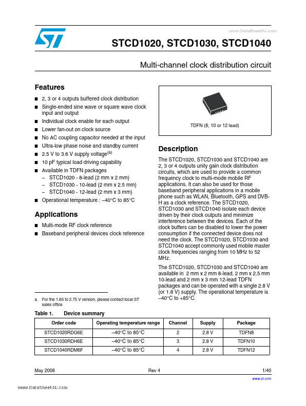
The STCD1020, STCD1030 and STCD1040 are 2, 3 or 4 outputs unity gain clock distribution circuits, which are used to provide a common frequency clock to multi-mode mobile RF applications.
| Part number | STCD1030 |
|---|---|
| Manufacturer | STMicroelectronics |
| File Size | 1.78 MB |
| Description | Multi-channel clock distribution circuit |
| Datasheet |
STCD1030 Datasheet
|
|
|
|
| Part Number | Description | Manufacturer |
|---|---|---|
| STC-013-000 | Transformer | YHDC |
| STC-R640 | high resolution CCD Color Cameras | KMIS |
| STC03DE150 | HYBRID EMITTER SWITCHED BIPOLAR TRANSISTOR | ST Microelectronics |
| STC03DE170 | HYBRID EMITTER SWITCHED BIPOLAR TRANSISTOR | ST Microelectronics |
| STC03DE170HP | Hybrid emitter switched bipolar transistor | ST Microelectronics |
| Part Number | Description |
|---|---|
| STCD1020 | Multi-channel clock distribution circuit |
| STCD1040 | Multi-channel clock distribution circuit |
| STC3100 | Battery monitor |
| STC3105 | Battery monitor |
| STC3115 | Gas gauge |
The following content is an automatically extracted verbatim text from the original manufacturer datasheet and is provided for reference purposes only.