Datasheet4U Logo Datasheet4U.com

STB7N52K3 - N-channel Power MOSFET

Datasheet Summary

Description

The new SuperMESH3™ series is obtained through the combination of a further fine tuning of ST's well established strip-based PowerMESH™ layout with a new optimization of the vertical structure.

Features

  • Type STB7N52K3 STD7N52K3 STF7N52K3 STP7N52K3 VDSS 525 V 525 V 525 V 525 V RDS(on) max < 0.98 Ω < 0.98 Ω < 0.98 Ω ID 6.3 A 6.3 A 6.3 A Pw 3 3 90 W 90 W 25 W 90 W 1 1 D²PAK DPAK < 0.98 Ω 6.3 A(1) 1. Limited by package.
  • 100% avalanche tested Extremely high dv/dt capability Gate charge minimized Very low intrinsic capacitances Improved diode reverse recovery characteristics Zener-protected Figure 1. 3 3 1 2 TO-220 1 2 TO-220FP Internal schematic diag.

📥 Download Datasheet

Datasheet preview – STB7N52K3

Datasheet Details

Part number STB7N52K3
Manufacturer STMicroelectronics
File Size 418.60 KB
Description N-channel Power MOSFET
Datasheet download datasheet STB7N52K3 Datasheet
Additional preview pages of the STB7N52K3 datasheet.
Other Datasheets by STMicroelectronics

Full PDF Text Transcription

Click to expand full text
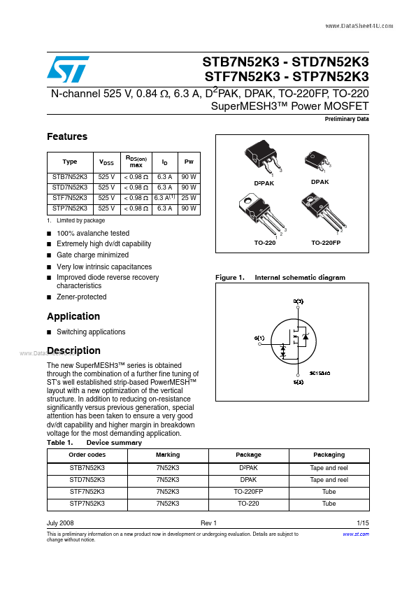
STB7N52K3 - STD7N52K3 STF7N52K3 - STP7N52K3 N-channel 525 V, 0.84 Ω, 6.3 A, D2PAK, DPAK, TO-220FP, TO-220 SuperMESH3™ Power MOSFET Preliminary Data Features Type STB7N52K3 STD7N52K3 STF7N52K3 STP7N52K3 VDSS 525 V 525 V 525 V 525 V RDS(on) max < 0.98 Ω < 0.98 Ω < 0.98 Ω ID 6.3 A 6.3 A 6.3 A Pw 3 3 90 W 90 W 25 W 90 W 1 1 D²PAK DPAK < 0.98 Ω 6.3 A(1) 1. Limited by package ■ ■ ■ ■ ■ ■ 100% avalanche tested Extremely high dv/dt capability Gate charge minimized Very low intrinsic capacitances Improved diode reverse recovery characteristics Zener-protected Figure 1. 3 3 1 2 TO-220 1 2 TO-220FP Internal schematic diagram Application ■ Switching applications www.DataSheet4U.
Published: |