STB50NF25
Features
Type
STP50NF25 STB50NF25
VDSS
250 V 250 V
RDS(on) Max
<0.069 Ω <0.069 Ω
ID PW
45 A 160 W 45 A 160 W
- 100% avalanche tested
- Gate charge minimized
- Low intrinsic capacitances
Application
Switching applications
Description
This Power MOSFET series realized with STMicroelectronics unique STrip FET™ process has specifically been designed to minimize onresistance and gate charge. It is therefore suitable as primary side switch allowing high efficiencies.
3 1
D²PAK
3 2 1
TO-220
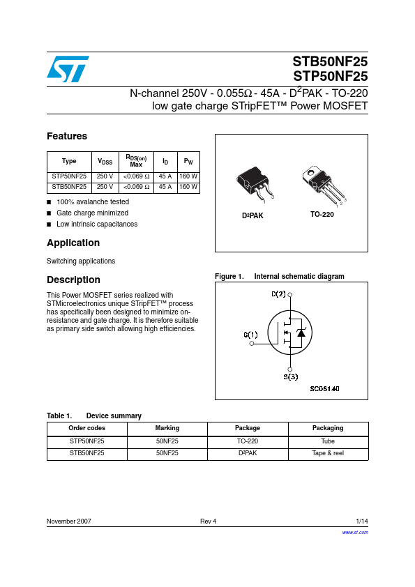
Figure 1. Internal schematic diagram
Table 1. Device summary Order codes STP50NF25 STB50NF25
Marking 50NF25 50NF25
Package TO-220 D²PAK
Packaging Tube
Tape & reel
November 2007
Rev 4
1/14
.st.
Contents
Contents
- STP50NF25
1 Electrical ratings
- -
- -
- -
- - . . . . 3 2...