STB50N25M5
Features
Type
VDSS
RDS(on) max
250 V < 0.075 Ω 28 A t(s)
- Amongst the best RDS(on)- area c
- High dv/dt capability du
- Excellent switching performance ro
- Easy to drive P
- 100% avalanche tested lete Application so
- Switching applications
- Ob Description t(s) This device is an N-channel MDmesh™ V Power
MOSFET based on an innovative proprietary c vertical process technology, which is bined u with STMicroelectronics’ well-known rod Power MESH™ horizontal layout structure. The resulting product has extremely low on-
P resistance, which is unmatched among siliconte based Power MOSFETs, making it especially le suitable for applications which require superior Obso power density and outstanding efficiency.
3 1
D²PAK
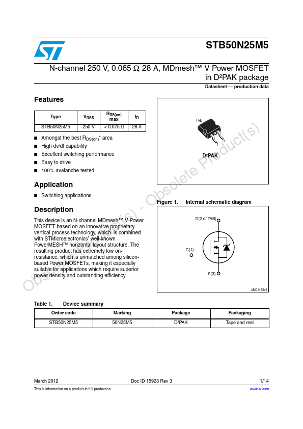
Figure 1. Internal schematic diagram
$OR4!"
' 3
!-V
Table 1. Device summary Order code STB50N25M5
Marking 50N25M5
Package D²PAK
Packaging Tape and reel
March 2012
This is information on a product in full production.
Doc ID...