D1047
Features
- High breakdown voltage VCEO = 140 V
- Typical ft = 20 MHz
- Fully characterized at 125 o C
Application
- Power supply
Description
The device is a NPN transistor manufactured using new Bi T-LA (Bipolar transistor for linear amplifier) technology. The resulting transistor shows good gain linearity behaviour.
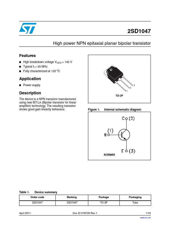
3 2 1
TO-3P
Figure 1. Internal schematic diagram
Table 1. Device summary Order code 2SD1047
April 2011
Marking 2SD1047
Package TO-3P
Doc ID 018729 Rev 1
Packaging Tube
1/10
.st.
Electrical ratings
1 Electrical ratings
Table 2. Absolute maximum ratings
Symbol
Parameter
VCBO VCEO VEBO
IC ICM Ptot Tstg TJ
Collector-base voltage (IE = 0) Collector-emitter voltage (IB = 0) Emitter-base voltage (IC = 0) Collector current Collector peak current (t P < 5 ms) Total dissipation at Tc = 25 °C Storage temperature Max. operating junction temperature
Table 3. Symbol Rthj-case
Thermal data Parameter
Thermal resistance junction-case ____max
2SD1047
Value 200 140
6 12 20...