The following content is an automatically extracted verbatim text
from the original manufacturer datasheet and is provided for reference purposes only.
View original datasheet text
®
74LVQ4066
QUAD BILATERAL SWITCH
s
s
s
s
s
s
s
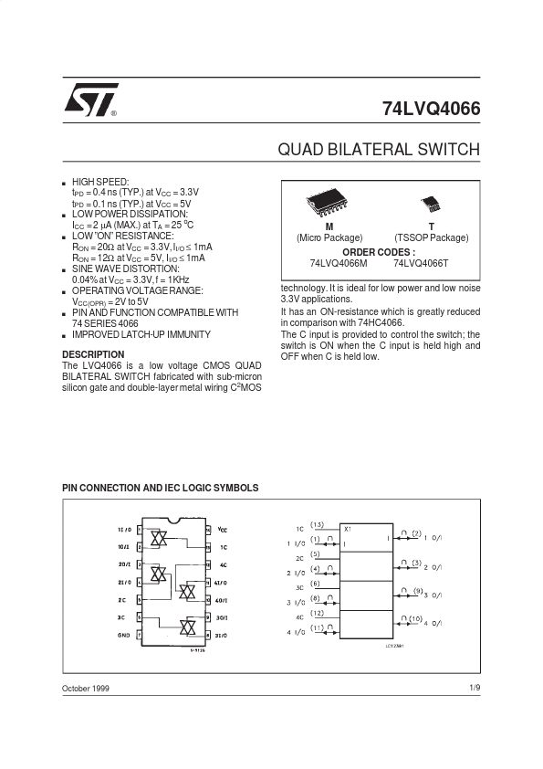
HIGH SPEED: tPD = 0.4 ns (TYP.) at VCC = 3.3V tPD = 0.1 ns (TYP.) at VCC = 5V LOW POWER DISSIPATION: ICC = 2 µA (MAX.) at TA = 25 oC LOW ”ON” RESISTANCE: RON = 20Ω at VCC = 3.3V, II/O ≤ 1mA RON = 12Ω at VCC = 5V, II/O ≤ 1mA SINE WAVE DISTORTION: 0.04% at VCC = 3.3V, f = 1KHz OPERATING VOLTAGE RANGE: VCC(OPR) = 2V to 5V PIN AND FUNCTION COMPATIBLE WITH 74 SERIES 4066 IMPROVED LATCH-UP IMMUNITY
M (Micro Package)
T (TSSOP Package)
ORDER CODES : 74LVQ4066M 74LVQ4066T technology. It is ideal for low power and low noise 3.3V applications. It has an ON-resistance which is greatly reduced in comparison with 74HC4066. The C input is provided to control the switch; the switch is ON when the C input is held high and OFF when C is held low.
 74LVQ4066 Datasheet