74ACT08
DESCRIPTION
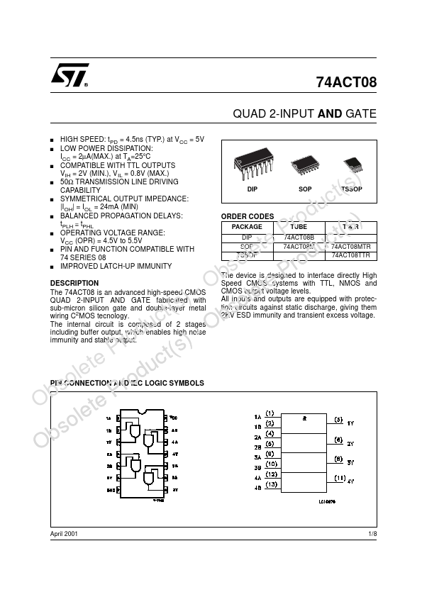
PIN No
1, 4, 9, 12 2, 5, 10, 13 3, 6, 8, 11
7 14
SYMBOL
1A to 4A 1B to 4B 1Y to 4Y
GND VCC
NAME AND FUNCTION
Data Inputs Data Inputs Data Outputs Ground (0V) Positive Supply Voltage
TRUTH TABLE
)L L L t(s L H L
HLL uc H H H rod )ABSOLUTE MAXIMUM RATINGS
P t(s Symbol
Parameter
Value
Unit lete uc VCC Supply Voltage
-0.5 to +7
V d VI DC Input Voltage
-0.5 to VCC + 0.5
V so ro VO DC Output Voltage
-0.5 to VCC + 0.5
V b PIIK DC Input Diode Current
± 20 m A
- O te IOK DC Output Diode Current
± 20 m A
) le IO DC Output Current
± 50 m A t(s so ICC or IGND DC VCC or Ground Current
± 200 m A c b Tstg Storage Temperature
-65 to +150
°C u OTL Lead Temperature (10 sec)
300 °C d -Absolute Maximum Ratings are those values beyond which damage to the device may occur. Functional operation under these conditions is ro )not implied.
P t(s REMENDED OPERATING CONDITIONS lete uc Symbol
Parameter so rod VCC Supply Voltage b PVI Input Voltage O te VO Output Voltage le Top...