Click to expand full text
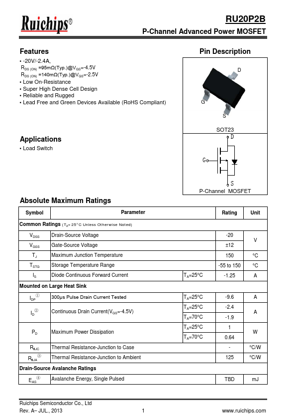
RU20P2B
P-Channel Advanced Power MOSFET
Features
• -20V/-2.4A,
RDS (ON) =95mΩ(Typ.)@VGS=-4.5V RDS (ON) =140mΩ(Typ.)@VGS=-2.5V
• Low On-Resistance • Super High Dense Cell Design • Reliable and Rugged • Lead Free and Green Devices Available (RoHS Compliant)
Applications
• Load Switch
Pin Description
D
G S
SOT23
D G
Absolute Maximum Ratings
Symbol
Parameter
Common Ratings (TA=25°C Unless Otherwise Noted)
VDSS
Drain-Source Voltage
VGSS
Gate-Source Voltage
TJ Maximum Junction Temperature
TSTG
Storage Temperature Range
IS Diode Continuous Forward Current
Mounted on Large Heat Sink
①
IDP
300μs Pulse Drain Current Tested
②
ID
Continuous Drain Current(VGS=-4.
 RU20P2B Datasheet