Applications
Power Management
Absolute Maximum Ratings
Symbol
times Parameter
g Common Ratings (TA=25°C Unless Otherwise Noted)
n VDSS
Drain-Source Voltage
he VGSS
Gate-Source Voltage
gs TJ
Maximum Junction Temperature
n TSTG
Storage Temperature Range
To IS
Diode Continuous F
The following content is an automatically extracted verbatim text
from the original manufacturer datasheet and is provided for reference purposes only.
View original datasheet text
sales.Mr.wang13826508770 www.sztssd.com
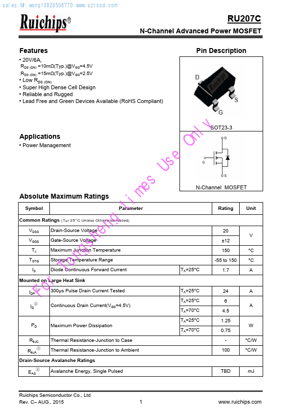
RU207C
N-Channel Advanced Power MOSFET
Features
• 20V/6A, RDS (ON) =10mΩ(Typ.)@VGS=4.5V RDS (ON) =15mΩ(Typ.)@VGS=2.5V • Low RDS (ON) • Super High Dense Cell Design • Reliable and Rugged • Lead Free and Green Devices Available (RoHS Compliant)
Pin Description
Applications
• Power Management
Absolute Maximum Ratings
Symbol
times Parameter
g Common Ratings (TA=25°C Unless Otherwise Noted)
n VDSS
Drain-Source Voltage
he VGSS
Gate-Source Voltage
gs TJ
Maximum Junction Temperature
n TSTG
Storage Temperature Range
To IS
Diode Continuous Forward Current
Mounted on Large Heat Sink
For IDP①
300μs Pulse Drain Current Tested
ID②
Continuous Drain Current(VGS=4.
 RU207C Datasheet