Click to expand full text
V103
TRIPLE 10-BIT LVDS TRANSMITTER FOR VIDEO
General Description
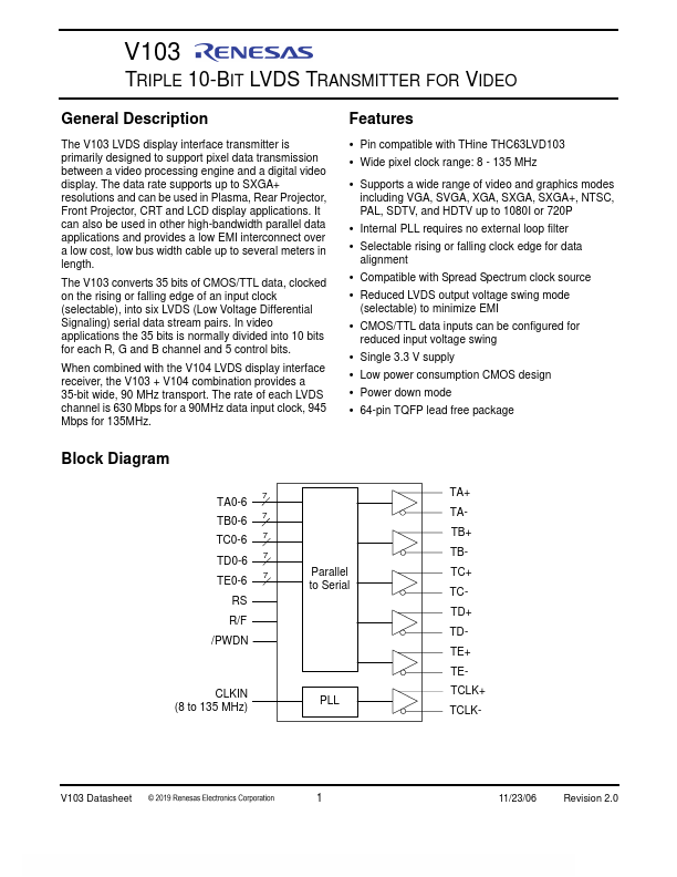
The V103 LVDS display interface transmitter is primarily designed to support pixel data transmission between a video processing engine and a digital video display. The data rate supports up to SXGA+ resolutions and can be used in Plasma, Rear Projector, Front Projector, CRT and LCD display applications. It can also be used in other high-bandwidth parallel data applications and provides a low EMI interconnect over a low cost, low bus width cable up to several meters in length.
The V103 converts 35 bits of CMOS/TTL data, clocked on the rising or falling edge of an input clock (selectable), into six LVDS (Low Voltage Differential Signaling) serial data stream pairs.
 V103 Datasheet