Datasheet Details
| Part number | SLG59M1599V |
|---|---|
| Manufacturer | Renesas |
| File Size | 373.78 KB |
| Description | Dual Load Switch |
| Datasheet |
 SLG59M1599V Datasheet SLG59M1599V Datasheet
|
|
|
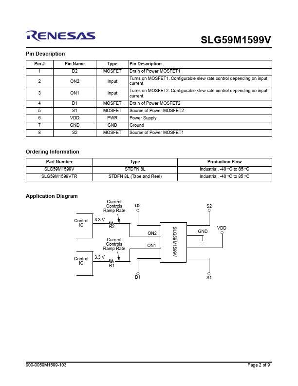
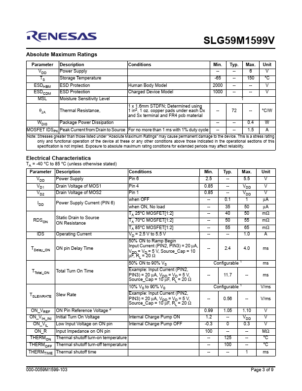
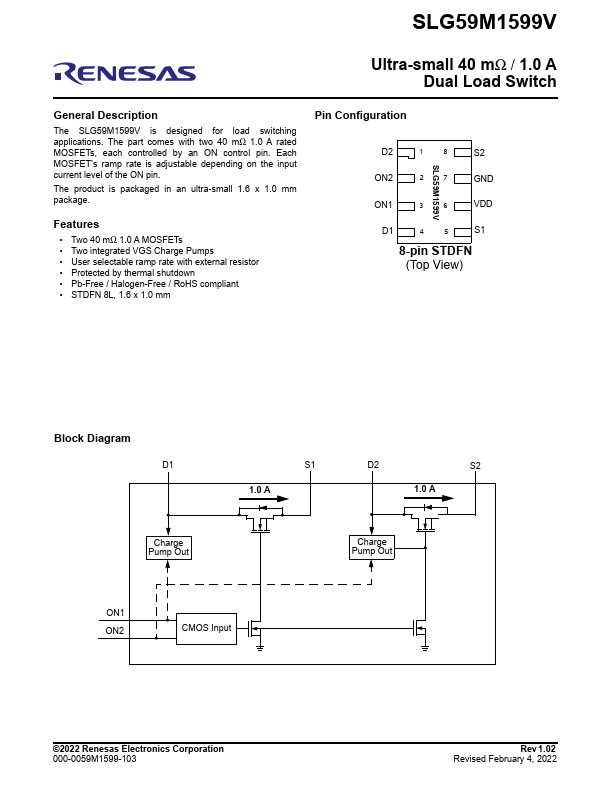
The SLG59M1599V is designed for load switching applications.
The part comes with two 40 mΩ 1.0 A rated MOSFETs, each controlled by an ON control pin.
Each MOSFET’s ramp rate is adjustable depending on the input current level of the ON pin.
| Part number | SLG59M1599V |
|---|---|
| Manufacturer | Renesas |
| File Size | 373.78 KB |
| Description | Dual Load Switch |
| Datasheet |
SLG59M1599V Datasheet
|
|
|
|