Click to expand full text
Preliminary Data Sheet
NP40N10YDF, NP40N10VDF, NP40N10PDF
100 V – 40 A – N-channel Power MOS FET Application: Automotive
R07DS0361EJ0201 Rev.2.01
May 13, 2013
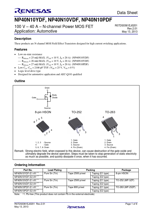
Description
These products are N-channel MOS Field Effect Transistors designed for high current switching applications.
Features
• Low on-state resistance ⎯ RDS(on) = 25 mΩ MAX. (VGS = 10 V, ID = 20 A) (NP40N10YDF) ⎯ RDS(on) = 26 mΩ MAX. (VGS = 10 V, ID = 20 A) (NP40N10VDF) ⎯ RDS(on) = 27 mΩ MAX. (VGS = 10 V, ID = 20 A) (NP40N10PDF)
• Low Ciss: Ciss = 2100 pF TYP. (VDS = 25 V, VGS = 0 V) • Logic level drive type • Designed for automotive application and AEC-Q101 qualified
Outline
Drain
Gate
Body Diode
Source
8-pin HSON
87 6 5
TO-252
4
TO-263
4
2 34 1
2 3
1
2
3 1
1, 2, 3 : Source 4 : Gate 5, 6, 7, 8: Drain
1. Gate 2.
 NP40N10YDF Datasheet