NP100P06PLG
Description
This product is P-channel MOS Field Effect Transistor designed for high current switching applications.
Features
- Super low on-state resistance : RDS(on) = 6.0 m Max. ( VGS = -10 V, ID = -50 A ) RDS(on) = 7.8 m Max. ( VGS = -4.5 V, ID = -50 A )
- Low input capacitance : Ciss = 15000 p F Typ.
- Built-in gate protection diode
- Designed for automotive application and AEC-Q101 qualified.
- Pb-free (This product does not contain Pb in the external electrode)
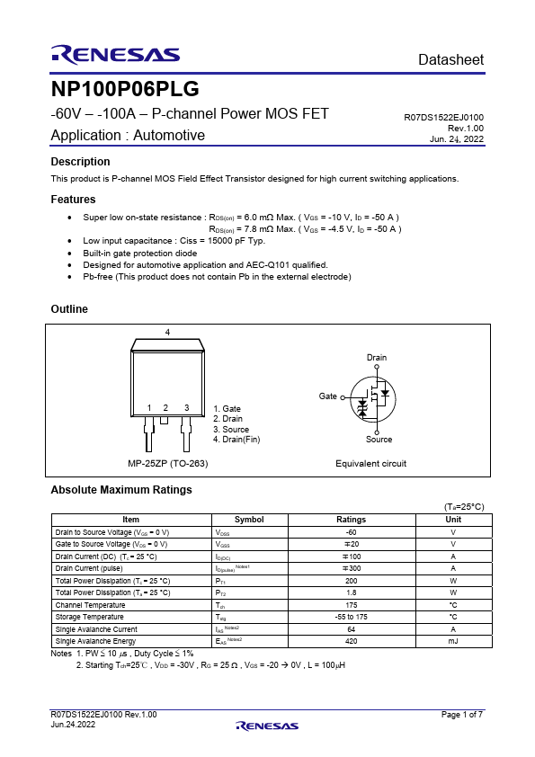
Outline
Drain
12 3
1. Gate 2. Drain 3. Source 4. Drain(Fin)
MP-25ZP (TO-263)
Absolute Maximum Ratings
Gate
Source
Equivalent circuit
Item
Symbol
Ratings
Drain to Source Voltage (VGS = 0 V)
VDSS
-60
Gate to Source Voltage (VDS = 0 V)
VGSS
20
Drain Current (DC) (Tc = 25 °C)
ID(DC)
100
Drain Current (pulse)
I Notes1
D(pulse)
300
Total Power Dissipation (Tc = 25 °C)
PT1
Total Power Dissipation (Ta = 25...