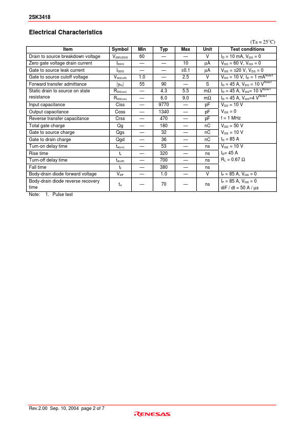
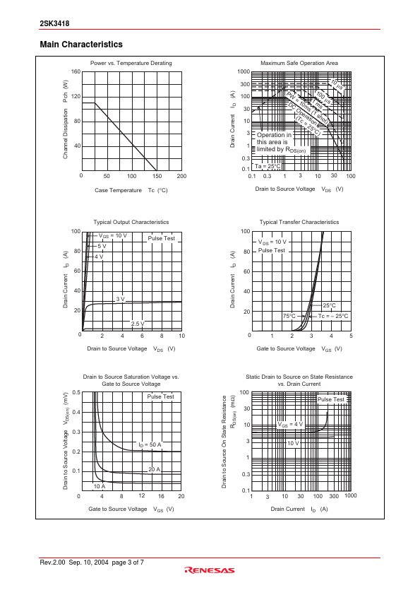
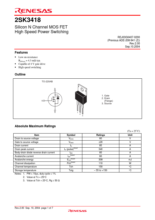
High speed switching
Outline
TO-220AB
D
G
S1 2 3
Absolute Maximum Ratings
Item Drain to source voltage Gate to source voltage Drain current Drain peak current Body-drain diode reverse drain current Avalanche current Avalanche energy Channel dissipation Channel temperature Storage temperature Notes: 1. PW ≤ 10µs, duty cycle ≤ 1%
2. Value at Tc = 25°C 3. Value at Tch = 25°C, Rg ≥ 50 Ω
Symbol
VDSS
V.
Note: Below is a high-fidelity text extraction (approx. 800 characters) for
K3418. For precise diagrams, and layout, please refer to the original PDF.
2SK3418 Silicon N Channel MOS FET High Speed Power Switching Features • Low on-resistance RDS(on) = 4.3 mΩ typ. • Capable of 4 V gate drive • High speed switching Outline...
View more extracted text
4.3 mΩ typ. • Capable of 4 V gate drive • High speed switching Outline TO-220AB D G S1 2 3 Absolute Maximum Ratings Item Drain to source voltage Gate to source voltage Drain current Drain peak current Body-drain diode reverse drain current Avalanche current Avalanche energy Channel dissipation Channel temperature Storage temperature Notes: 1. PW ≤ 10µs, duty cycle ≤ 1% 2. Value at Tc = 25°C 3. Value at Tch = 25°C, Rg ≥ 50 Ω Symbol VDSS VGSS ID ID (pulse)Note1 IDR IAPNote3 EARNote3 PchNote2 Tch Tstg REJ03G0407-0200 (Previous ADE-208-941 (Z)) Rev.2.00 Sep.10.2004 1. Gate 2. Drain (Flange) 3.
 K3418 Datasheet