Suitable for switching regulator and DC-DC converter
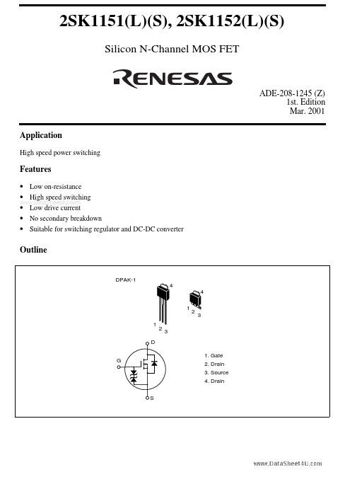
Outline
DPAK-1 4 4 1 1 D G 1. Gate 2. Drain 3. Source 4. Drain S
2
3
2 3
2SK1151(L)(S), 2SK1152(L)(S)
Absolute Maximum Ratings (Ta = 25°C)
Item Drain to source voltage 2SK1151 2SK1152 Gate to source voltage Drain current Drain peak current Body to drain diode reverse drain current Channel d.
Note: Below is a high-fidelity text extraction (approx. 800 characters) for
K1152. For precise diagrams, and layout, please refer to the original PDF.
To all our customers Regarding the change of names mentioned in the document, such as Hitachi Electric and Hitachi XX, to Renesas Technology Corp. The semiconductor opera...
View more extracted text
ic and Hitachi XX, to Renesas Technology Corp. The semiconductor operations of Mitsubishi Electric and Hitachi were transferred to Renesas Technology Corporation on April 1st 2003. These operations include microcomputer, logic, analog and discrete devices, and memory chips other than DRAMs (flash memory, SRAMs etc.) Accordingly, although Hitachi, Hitachi, Ltd., Hitachi Semiconductors, and other Hitachi brand names are mentioned in the document, these names have in fact all been changed to Renesas Technology Corp. Thank you for your understanding. Except for our corporate trademark, logo and www.DataSheet4U.
 K1152 Datasheet