Click to expand full text
DATASHEET
1.5V LOW-POWER WIDE-RANGE FREQUENCY CLOCK DRIVER
ICS98UAE877A
Description
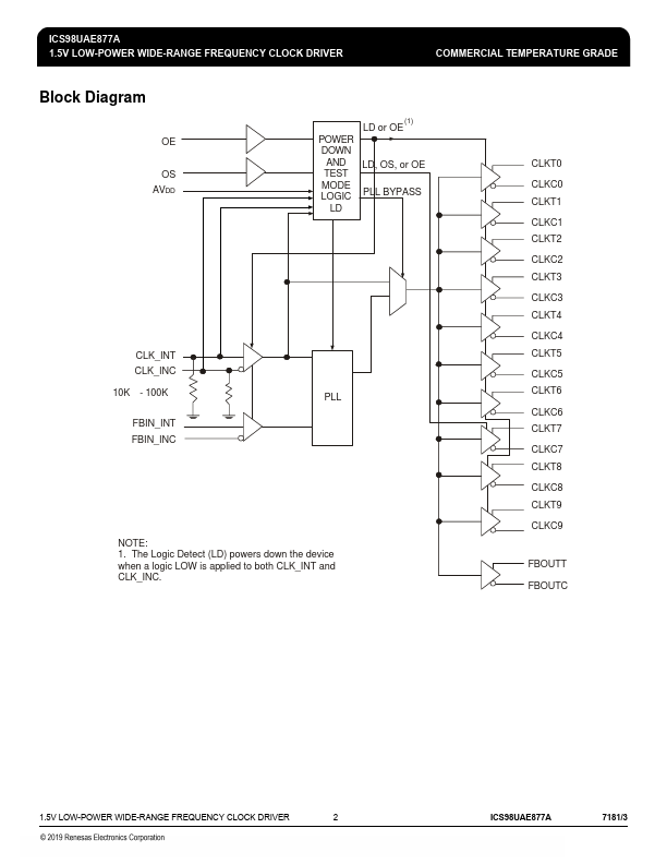
The PLL clock buffer, ICS98UAE877A, is designed for a VDDQ of 1.5V, an AVDD of 1.5V and differential data input and output levels.
ICS98UAE877A is a zero delay buffer that distributes a differential clock input pair (CLK_INT, CLK_INC) to ten differential pair of clock outputs (CLKT[0:9], CLKC[0:9]) and one differential pair feedback clock outputs (FB_OUTT, FBOUTC). The clock outputs are controlled by the input clocks (CLK_INT, CLK_INC), the feedback clocks (FB_INT, FB_INC), the LVCMOS program pins (OE, OS) and the Analog Power input (AVDD). When OE is low, the outputs (except FB_OUTT/FB_OUTC) are disabled while the internal PLL continues to maintain its locked-in frequency.
 ICS98UAE877A Datasheet