Click to expand full text
ICS95V1 5 7
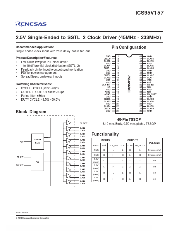
2.5V Single-Ended to SSTL_2 Clock Driver (45MHz - 233MHz)
Recommended Application: Single-ended clock input with zero delay board fan out
Product Description/Features: • Low skew, low jitter PLL clock driver • 1 to 10 differential clock distribution (SSTL_2) • Feedback pin for input to output synchronization • PD# for power management • Spread Spectrum tolerant inputs
Switching Characteristics: • CYCLE - CYCLE jitter: <60ps • OUTPUT - OUTPUT skew: <60ps • Period jitter: ±30ps • DUTY CYCLE: 49.5% - 50.5%
Pin Configuration
Block Diagram
48-Pin TSSOP
6.10 mm. Body, 0.50 mm. pitch = TSSOP
Functionality
INPUTS
OUTPUTS
AVDD PD# CLK_INT CLKT CLKC FB_OUTT
PLL State
GND H
L
LH
L
Bypassed/off
GND H
H
HL
2.5V (nom)
L
L
ZZ
2.5V (nom)
L
H
ZZ
2.
 ICS95V157 Datasheet