Datasheet Details
| Part number | ICS557GI-06LF |
|---|---|
| Manufacturer | Renesas |
| File Size | 287.74 KB |
| Description | 2 TO 4 DIFFERENTIAL PCIE GEN1 CLOCK MUX |
| Datasheet |
 ICS557GI-06LF Datasheet ICS557GI-06LF Datasheet
|
|
|
Download the ICS557GI-06LF datasheet PDF. This datasheet also covers the ICS557-06 variant, as both devices belong to the same 2 to 4 differential pcie gen1 clock mux family and are provided as variant models within a single manufacturer datasheet.
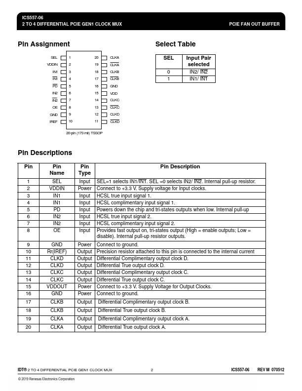
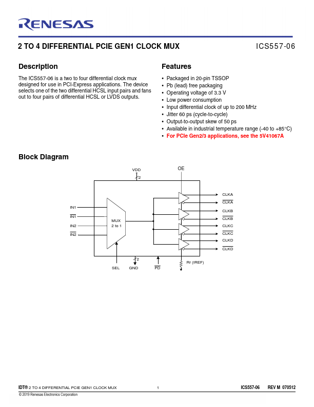
The ICS557-06 is a two to four differential clock mux designed for use in PCI-Express applications.
The device selects one of the two differential HCSL input pairs and fans out to four pairs of differential HCSL or LVDS outputs.
| Part number | ICS557GI-06LF |
|---|---|
| Manufacturer | Renesas |
| File Size | 287.74 KB |
| Description | 2 TO 4 DIFFERENTIAL PCIE GEN1 CLOCK MUX |
| Datasheet |
ICS557GI-06LF Datasheet
|
|
|
|
| Part Number | Description | Manufacturer |
|---|---|---|
| ICS557-01 | PCI-EXPRESS CLOCK SOURCE | ICST |
| ICS557-03 | spread spectrum clock generator | IDT |
| ICS557-05A | Quad Differential PCI-Express Clock Source | ICST |
| ICS557-06 | ONE TO FOUR HCSL CLOCK BUFFER | ICST |
| ICS557-08 | 2:1 MULTIPLEXER CHIP | ICST |
| Part Number | Description |
|---|---|
| ICS557GI-03LF | 2 OUTPUT PCI-EXPRESS GEN1 CLOCK SOURCE |
| ICS557GI-08LF | 2:1 MULTIPLEXER |
| ICS557G-03LF | 2 OUTPUT PCI-EXPRESS GEN1 CLOCK SOURCE |
| ICS557G-06LF | 2 TO 4 DIFFERENTIAL PCIE GEN1 CLOCK MUX |
| ICS557G-08LF | 2:1 MULTIPLEXER |