Click to expand full text
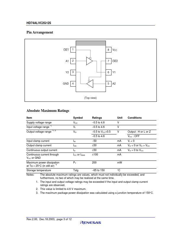
HD74ALVC2G125
Dual Bus Buffer with 3-state Output
REJ03D0171–0200Z (Previous ADE-205-621A (Z))
Rev.2.00 Dec.18.2003
Description
The HD74ALVC2G125 has dual bus buffer with 3-state output in an 8 pin package. Output is disabled when the associated output enable (OE) input is high. To ensure the high impedance state during power up or power down, OE should be connected to VCC through a pull-up resistor; the minimum value of the resistor is determined by the current sinking capability of the driver. Low voltage and high-speed operation is suitable for the battery powered products (e.g., notebook computers), and the low power consumption extends the battery life.
Features
• The basic gate function is lined up as Renesas uni logic series.
 HD74ALVC2G125 Datasheet