Datasheet Details
| Part number | 553S |
|---|---|
| Manufacturer | Renesas |
| File Size | 952.43 KB |
| Description | Low Skew 1 to 4 Clock Buffer |
| Datasheet |
 553S Datasheet 553S Datasheet
|
|
|
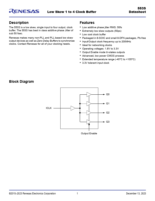
The 553S is a low skew, single input to four output, clock buffer.
The 553S has best in class additive phase Jitter of sub 50 fsec.
Renesas makes many non-PLL and PLL based low skew output devices as well as Zero Delay Buffers to synchronize clocks.
| Part number | 553S |
|---|---|
| Manufacturer | Renesas |
| File Size | 952.43 KB |
| Description | Low Skew 1 to 4 Clock Buffer |
| Datasheet |
553S Datasheet
|
|
|
|
Note: Below is a high-fidelity text extraction (approx. 800 characters) for 553S. For precise diagrams, and layout, please refer to the original PDF.
Low Skew 1 to 4 Clock Buffer 553S Datasheet Description The 553S is a low skew, single input to four output, clock buffer. The 553S has best in class additive phase Jitte...
| Brand Logo | Part Number | Description | Manufacturer |
|---|---|---|---|
| 553S | Low Skew 1 to 4 Clock Buffer | IDT | |
| 553-xxxx-xxx | LED Array | Dialight | |
| 5532 | Internally Compensated Dual Low Noise Operational Amplifier | NXP |
| Part Number | Description |
|---|---|
| 553MILF | LOW SKEW 1 TO 4 CLOCK BUFFER |
| 553MLF | LOW SKEW 1 TO 4 CLOCK BUFFER |