Click to expand full text
2SJ574
Silicon P Channel MOS FET High Speed Switching
Features
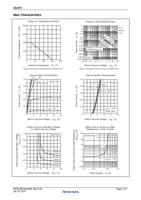
• Low on-resistance RDS = 1.1 Ω typ. (VGS = –10 V, ID = –150 mA) RDS = 2.2 Ω typ. (VGS = –4 V, ID = –150 mA)
• 4 V gate drive device. • Small package (MPAK)
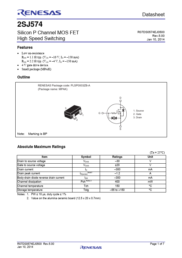
Outline
RENESAS Package code: PLSP0003ZB-A (Package name: MPAK)
Note: Marking is BP
3 G
1 2
Preliminary Datasheet
R07DS0574EJ0500 Rev.5.00
Jan 10, 2014
D 1. Source 2. Gate 3. Drain
S
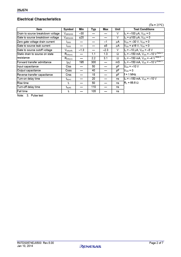
Absolute Maximum Ratings
Item
Symbol
Drain to source voltage Gate to source voltage Drain current Drain peak current Body-drain diode reverse drain current Channel dissipation
VDSS
VGSS
ID ID(pulse)Note1
IDR Pch Note 2
Channel temperature
Tch
Storage temperature
Tstg
Notes: 1. PW ≤ 10 µs, duty cycle ≤ 1%
2. Value on the alumina ceramic board (12.5 x 20 x 0.
 2SJ574 Datasheet