The following content is an automatically extracted verbatim text
from the original manufacturer datasheet and is provided for reference purposes only.
View original datasheet text
www.DataSheet4U.com
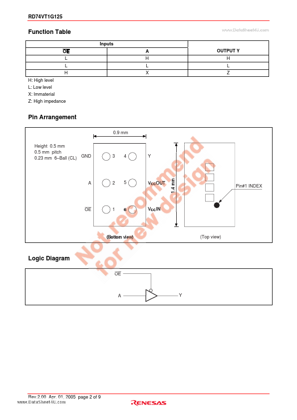
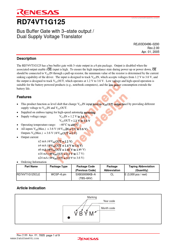
RD74VT1G125
Bus Buffer Gate with 3–state output / Dual Supply Voltage Translator
REJ03D0496–0200 Rev.2.00 Apr. 01, 2005
Description
The RD74VT1G125 has a bus buffer gate with 3–state output in a 6 pin package. Output is disabled when the associated output enable (OE) input is high. To ensure the high impedance state during power up or power down, OE should be connected to VCCIN through a pull-up resistor, the minimum value of the resistor is determined by the current sinking capability of the driver. The input is designed to track VCCIN, which accepts voltages from 1.2 V to 3.6 V, and the output is designed to track VCCOUT, which operates at 1.2 V to 3.6 V. Low voltage and high-speed operation is suitable for the battery powered products (e.g.
 RD74VT1G125 Datasheet